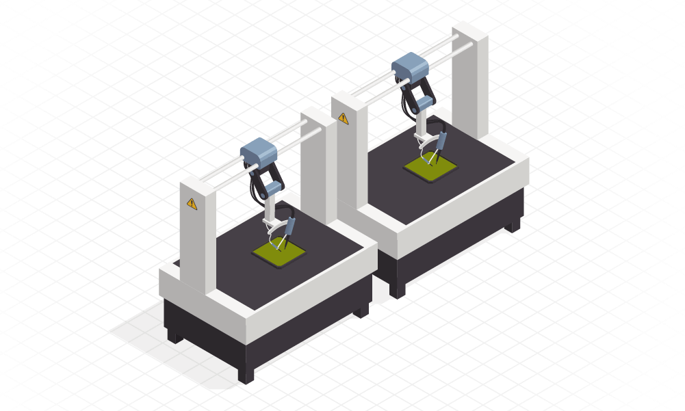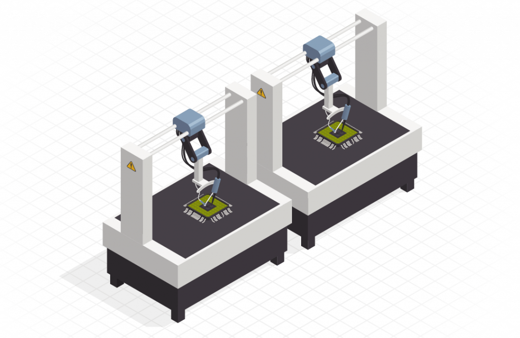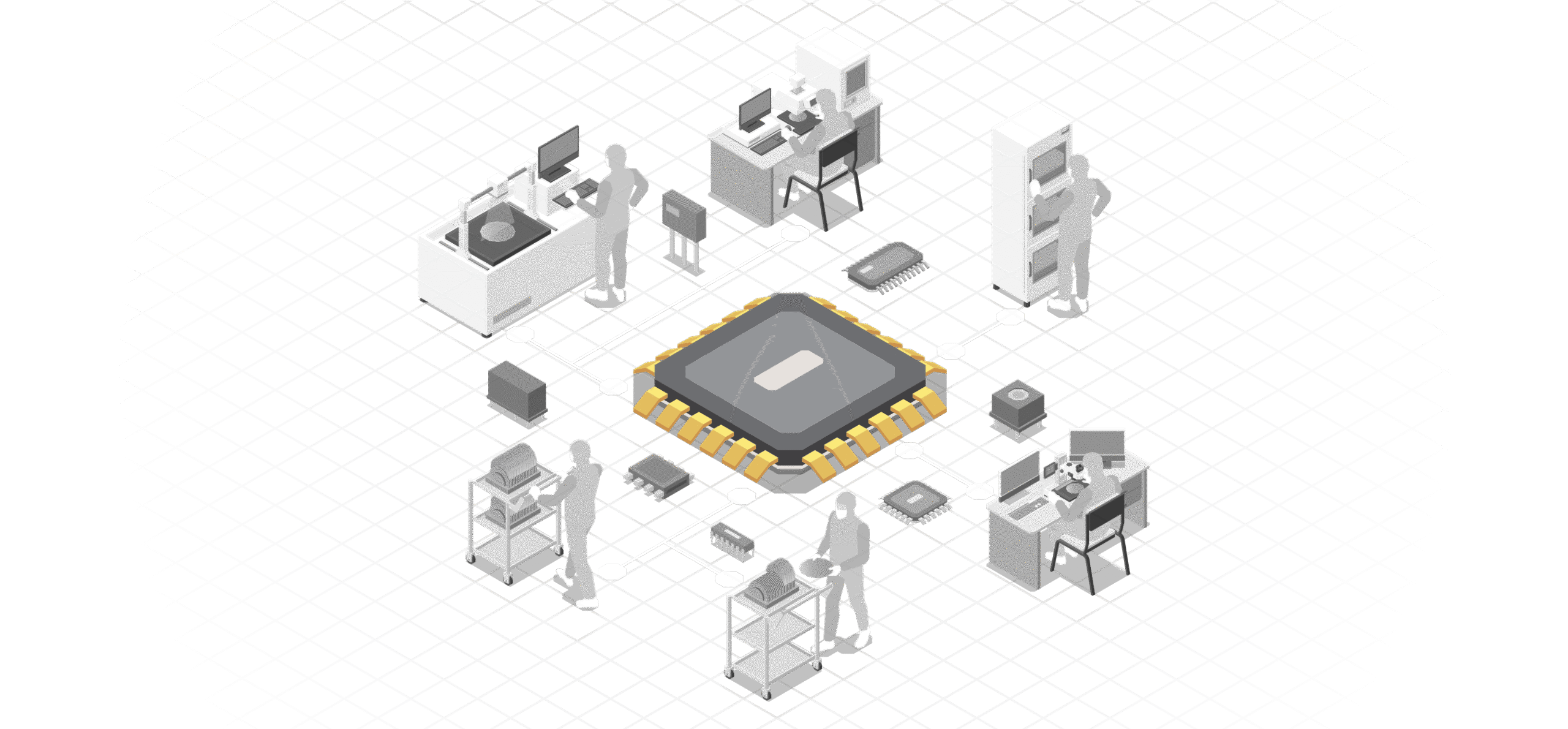
Walk into a semiconductor fabrication plant in 2025 and you’ll see something that looks more like a science fiction set than a factory. Robots glide across spotless cleanrooms, wafers are carried through vacuum-sealed chambers, and machines whisper in precision rhythms. Each wafer that enters the fab is a canvas on which billions of transistors will be etched, stacked, and polished.
But behind this incredible story of machines lies a truth: fabs are under immense pressure. Every new generation of chips is harder to make. Transistors are now so small that thousands could fit across the width of a human hair. Processes that were once manageable by traditional inspection are now too complex, too fast, and too unforgiving. A single microscopic flaw, smaller than a virus, can ripple through thousands of wafers and cost millions of dollars in yield losses.
This is why 2025 is different. This is the year when inspection in fabs shifts decisively from being a checkpoint to being the nervous system of manufacturing. Computer vision, paired with deep learning and automation, is no longer optional, it’s essential. This rise of Vision AI in wafer fabs is one of the defining Semiconductor fab trends 2025, transforming how defects are found, predicted, and prevented.
In the sections ahead, we’ll explore why inspection matters more than ever, how AI is reshaping it, the trends driving the change, and what the fab of the future looks like.
Why Vision AI Matters Now
Semiconductor fabs have always been about precision. But the level of precision required in 2025 is unlike anything seen before.
Each chip today may contain over 100 billion transistors. The photomasks used to print patterns are more complex than city maps. Layers stack one on top of another, sometimes more than 80 deep, each requiring flawless alignment. And as architectures like 3D ICs and chiplets become more common, even vertical stacking must be perfect.
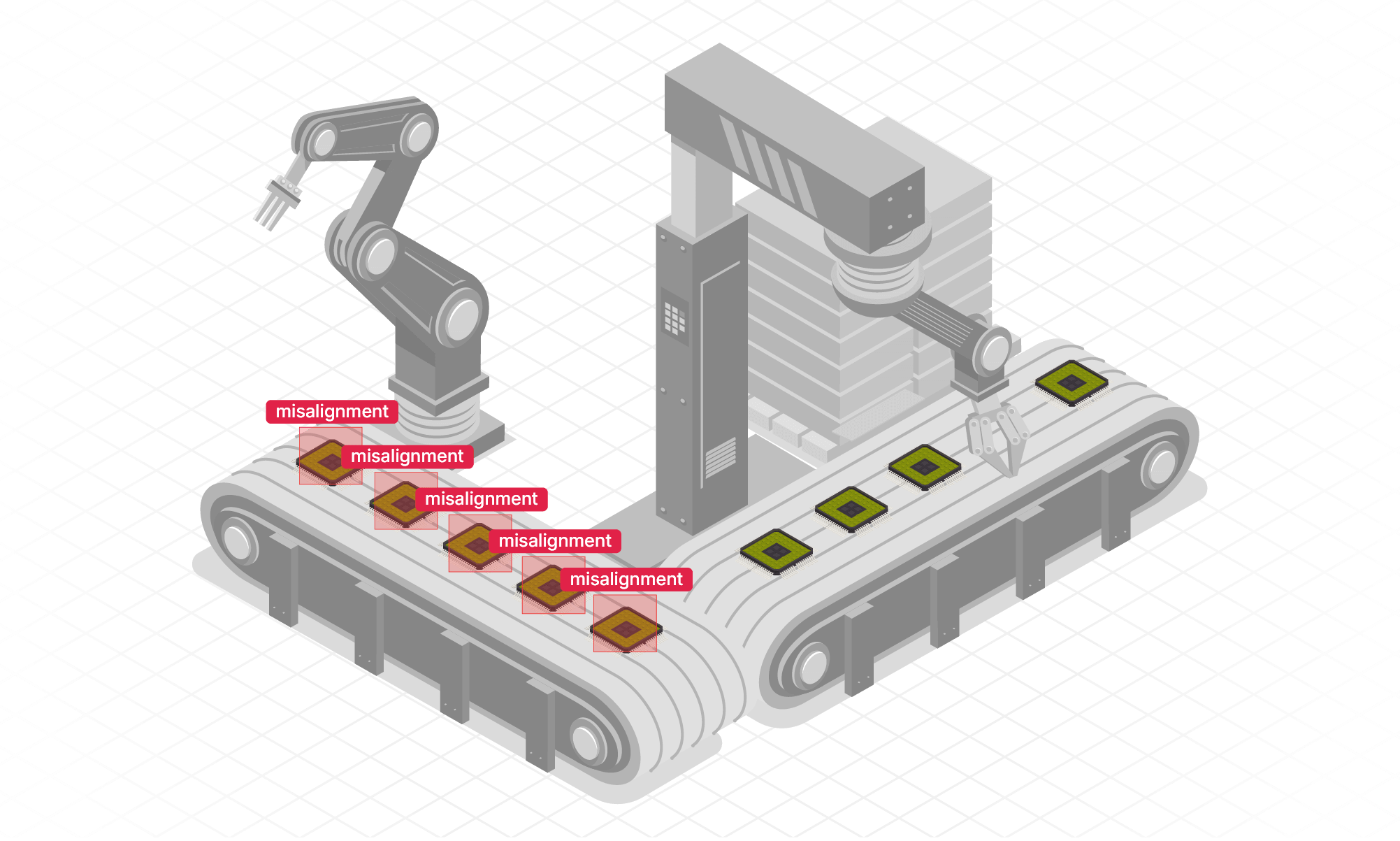
The problem is that traditional inspection tools, optical microscopes, rule-based automation, or manual review, cannot keep up. They either miss tiny defects or overwhelm engineers with false alarms. Worse, they are reactive: they tell you a defect has occurred, but not how to stop it from happening again.
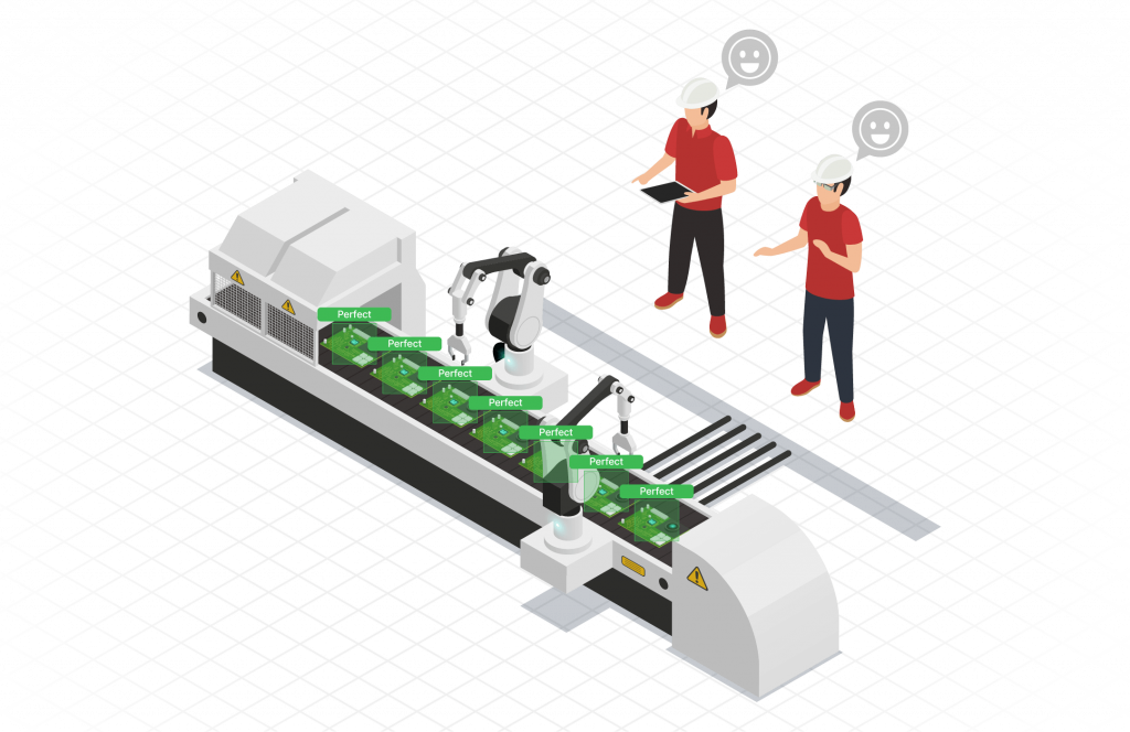
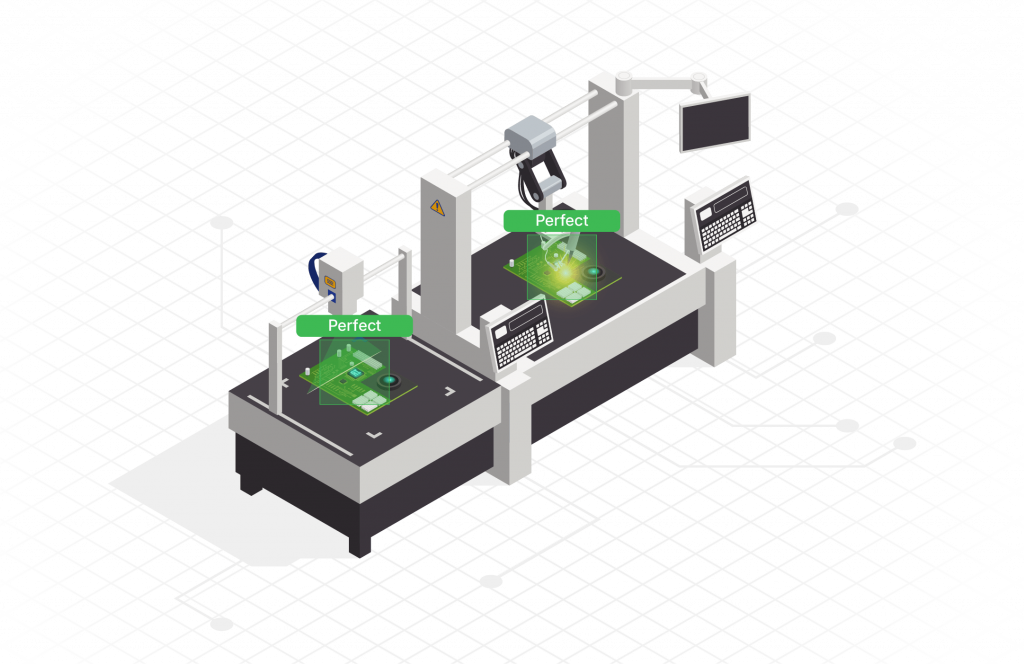
By contrast, AI inspection semiconductor systems work differently. They don’t just scan wafers; they learn from them. They analyze massive datasets of wafer images, detect patterns humans can’t see, and predict issues before they cascade. They can operate in real time, ensuring that problems are corrected on the fly rather than after the fact.
In short: AI doesn’t just give fabs new tools. It gives them new eyes, and in many cases, a new brain.
Key Vision AI & Inspection Trends in 2025
Now let’s explore the defining trends of 2025, how inspection technologies powered by AI are rewriting the rules of semiconductor manufacturing.
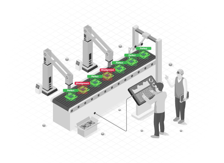
1. Predictive Defect Detection
In older fabs, inspection was like looking in the rearview mirror: you saw defects after they happened. But by then, dozens of wafers were already damaged.
In 2025, inspection has become predictive. By analyzing patterns across thousands of wafers, AI systems can forecast problems before they appear. For example, subtle changes in slurry flow during CMP polishing can signal erosion risks. Tiny irregularities in plasma glow can warn of etching drift. AI systems catch these warning signs and alert operators, or even adjust processes automatically, before defects spread.
This shift to predictive defect detection is saving fabs millions each year. Instead of reacting to yield losses, fabs now prevent them. It’s like moving from a doctor who treats illnesses to one who predicts them and keeps you healthy.
2. Edge AI in Semiconductor Inspection
Inspection creates enormous amounts of image data. A single wafer scan can generate terabytes of information. Sending all of this to cloud servers for processing is slow and risky.
That’s why in 2025, more fabs are deploying Edge AI in semiconductor lines. Processing happens directly at the tool, right where wafers are polished, etched, or patterned. This reduces latency, ensures immediate feedback, and keeps sensitive design data secure.
For time-critical processes like etching, CMP, or resist coating, edge AI is a game-changer. Decisions that once took minutes now happen in seconds.
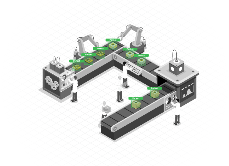
3. Fab Automation Trends
Fabs are also moving toward greater automation. But automation in 2025 isn’t just about robots moving wafers, it’s about inspection systems that take corrective action on their own.
These fab automation trends include closed-loop systems. Imagine CMP polishing: if AI vision detects early signs of dishing, it can automatically adjust pad pressure or slurry flow. In lithography, if overlay drift is detected, exposure parameters can be corrected instantly.
This automation turns fabs into self-healing systems, reducing reliance on manual intervention and cutting downtime.
4. Multi-Stage Vision AI Integration
Until recently, fabs treated inspection as siloed steps. There was one system for photomasks, another for CMP, another for packaging. Each step generated data, but that data rarely connected.
Now, AI is integrating inspection across the entire fab. Results from photomask inspection inform wafer-level monitoring. CMP data feeds into packaging checks. By connecting dots across the process, fabs can find root causes faster and optimize workflows holistically.
This multi-stage integration is a stepping stone to future semiconductor inspection, where data from across fabs is unified into one intelligent system.
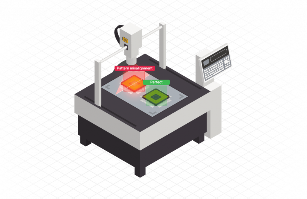
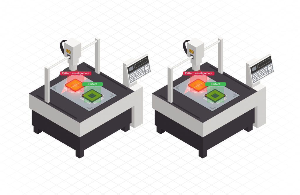
5. Smarter Defect Classification
Another big trend in 2025 is smarter classification. Instead of simply labeling a wafer as good or bad, AI systems categorize defects precisely: scratches, pits, voids, erosion, bubbles.
Knowing the type of defect helps fabs respond quickly. A scratch might mean maintenance on pads. A void could indicate process gas instability. Erosion might require slurry adjustments. By giving context, AI turns inspection from a red flag into actionable insight.
This is one of the quiet revolutions of 2025, inspection isn’t just about detection anymore. It’s about diagnosis.
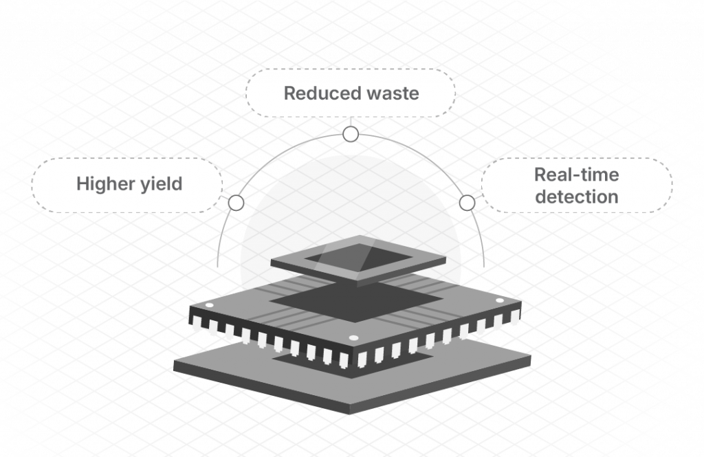
6. Sustainability and Yield Optimization
Sustainability is also shaping inspection trends. Fabs consume huge amounts of water, chemicals, and energy. Every defective wafer means wasted resources.
By improving yields and reducing scrap, Vision AI helps fabs lower both costs and environmental impact. Some fabs report that AI monitoring of CMP and resist coating cut chemical usage by 10-15%. Others note that predictive maintenance reduced downtime, saving both energy and materials.
In an industry under pressure to balance growth with responsibility, this is a major win.
Challenges in 2025
Even with these advances, challenges remain.
- Data volume: Each wafer generates terabytes of inspection images. Managing and analyzing this at scale requires hybrid architectures combining edge and cloud.
- Integration: Connecting AI inspection with MES, yield management, and process control systems is complex but essential.
- IP security: Fabs must protect design data when training AI models.
- Continuous retraining: AI models must evolve as new nodes, materials, and defect types emerge.
Despite these hurdles, investment is accelerating. Fabs know that without Vision AI, they risk falling behind.
The Future of Semiconductor Inspection
Looking ahead, inspection will become the fabric of fabs, not just a feature.
Future semiconductor inspection will be:
- Proactive: predicting and preventing defects, not just finding them.
- Integrated: linking data across tools, fabs, and even global supply chains.
- Autonomous: working hand in hand with robots and process tools to create truly self-healing fabs.
- Sustainable: cutting waste and optimizing resources.
The vision is a fab where defect-driven yield loss is near zero, where wafers move through processes guided by intelligent systems that see everything and act instantly.
At WebOccult, we see inspection as more than quality control, it’s the foundation of semiconductor automation.
Our solutions combine deep learning, edge processing, and seamless integration to give fabs real-time insights at every step. We help manufacturers implement AI inspection semiconductor systems that predict problems, enable closed-loop control, and scale across nodes.
Whether it’s photomask inspection, CMP monitoring, overlay accuracy, or packaging validation, our vision based inspection platforms are designed for precision, adaptability, and reliability.
As fabs evolve into smart fabs, WebOccult is here to help them achieve higher yields, lower costs, and greater confidence in every wafer produced.
Conclusion
The semiconductor industry in 2025 is both more exciting and more demanding than ever. Chips are powering AI, 5G, autonomous vehicles, and more. But manufacturing them has never been harder. Traditional inspection cannot keep up.
Vision AI in wafer fabs has become the guardian of this new era. It predicts defects, enables real-time corrections, and connects data across processes. It reduces waste, improves yield, and makes fabs smarter and more sustainable.
In the landscape of Semiconductor fab trends 2025, inspection is not a footnote, it’s the headline. It is the key to unlocking smaller nodes, advanced architectures, and reliable supply chains.
At WebOccult, we believe that in the race for precision, inspection is not just about what you see, it’s about what you can predict, prevent, and perfect. That is the promise of Vision AI, and that is the future of semiconductor manufacturing.