Fuel is one of the largest recurring expenses in container yard operations, yet it is often treated as a fixed cost rather than a controllable variable. Most operators focus on throughput, turnaround time, and capacity utilization, but overlook how daily inefficiencies quietly inflate fuel consumption. The truth is straightforward: fuel costs are rarely high because of volume alone. They rise because of poor visibility, unstructured movement, and under-monitored equipment behavior.
Reducing fuel costs by 15-20% is not unrealistic. It requires a shift in how yard operations are observed, measured, and managed, especially when it comes to Container Handling Equipment (CHE). When movement becomes intentional and equipment usage is guided by real-time data, fuel stops being a silent expense and becomes an optimizable metric.
The Hidden Drain on Profits
Fuel losses in a container yard are rarely obvious. They do not appear as a single large expense spike; instead, they accumulate through everyday inefficiencies that go unnoticed.
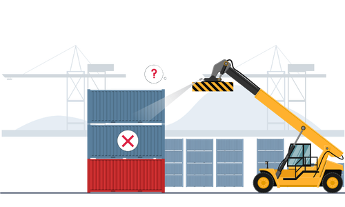
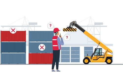
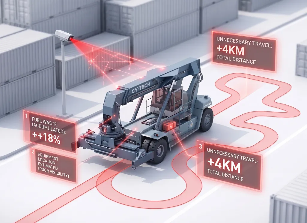
One of the biggest contributors is unnecessary movement. When container locations are unclear or mismanaged, equipment operators spend extra time driving across the yard to locate, reposition, or verify containers. These additional trips may seem minor individually, but over the course of a day, they significantly increase fuel consumption.
Idle time is another major factor. Equipment that remains switched on while waiting for instructions, queue clearance, or task allocation continues to consume fuel without contributing to productivity. In yards with poor coordination, idle time can account for a surprisingly large portion of total fuel usage.
Then there is the issue of rework. Misplaced containers or incorrect stacking often require additional handling cycles. Each extra lift, shift, or relocation consumes fuel, increases wear on equipment, and slows down overall operations.
These inefficiencies are rarely tracked in detail, which is why they remain hidden. However, when aggregated, they represent a substantial drain on profitability.
Focusing on the Equipment
Many yard optimization strategies focus heavily on containers, where they are placed, how quickly they move, and how efficiently space is used. While this is important, it only tells half the story.
The real drivers of fuel consumption are the machines moving those containers.
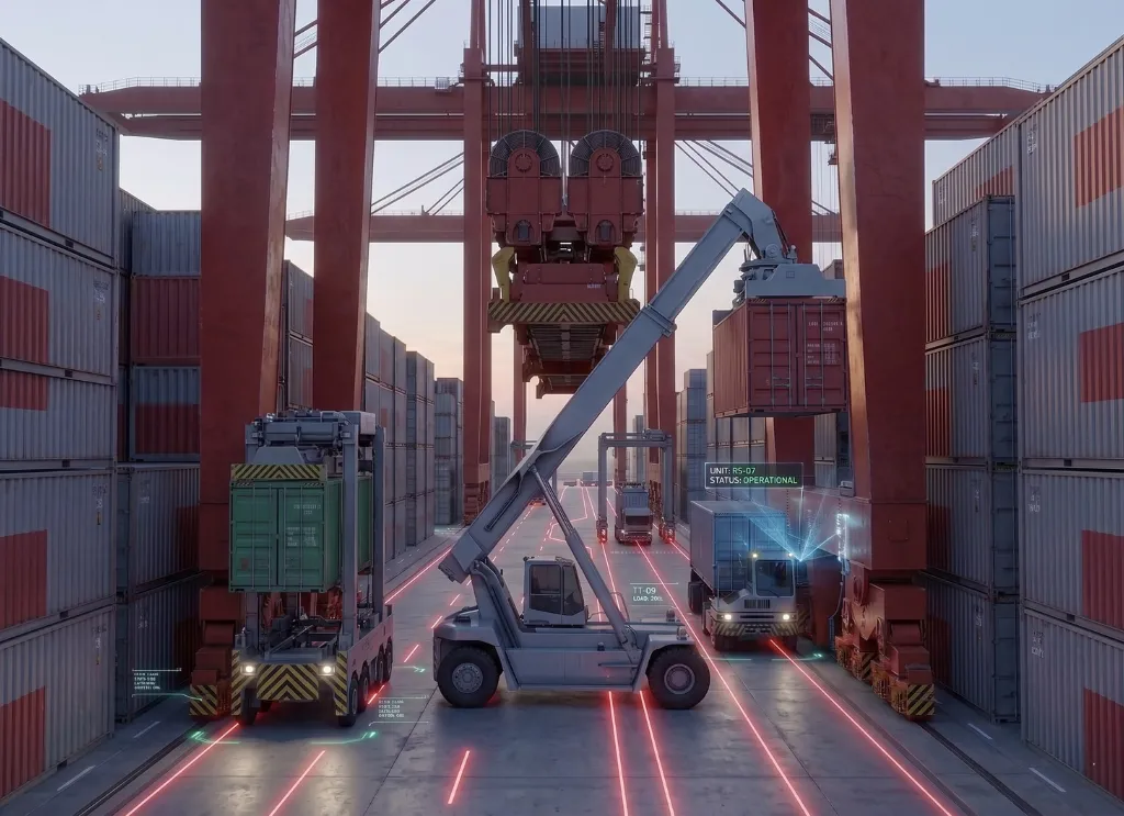
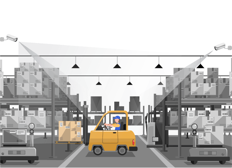
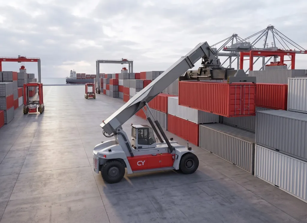
Container Handling Equipment, whether it includes reach stackers, forklifts, rubber-tyred gantry cranes, or terminal tractors, operates continuously throughout the yard. Each movement, each idle minute, and each maintenance lapse directly impacts fuel usage.
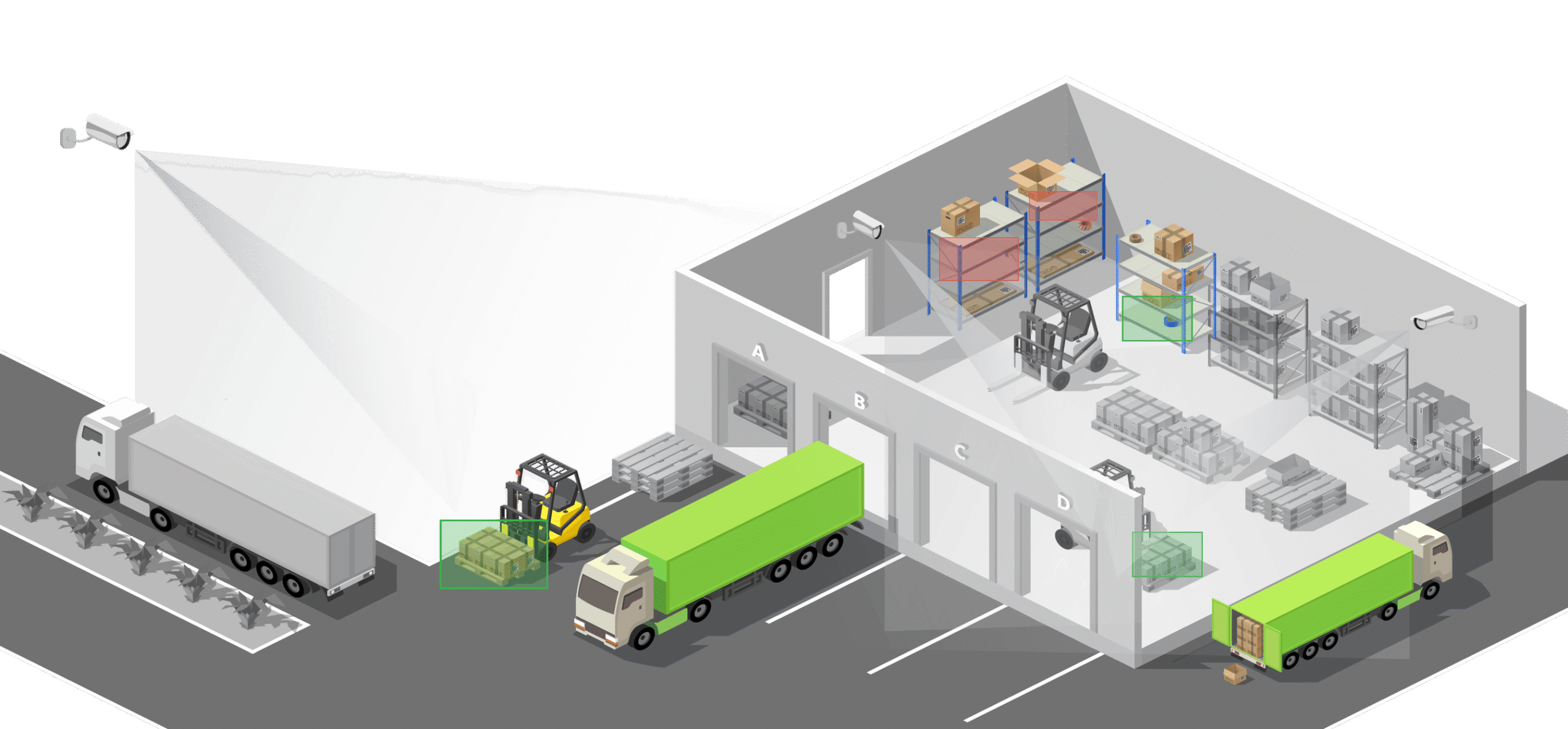
Tracking CHE location is critical. Without knowing where equipment is at any given moment, it becomes difficult to assign tasks efficiently. Operators may be sent across long distances for jobs that could have been handled by closer machines. This leads to unnecessary travel and higher fuel burn.
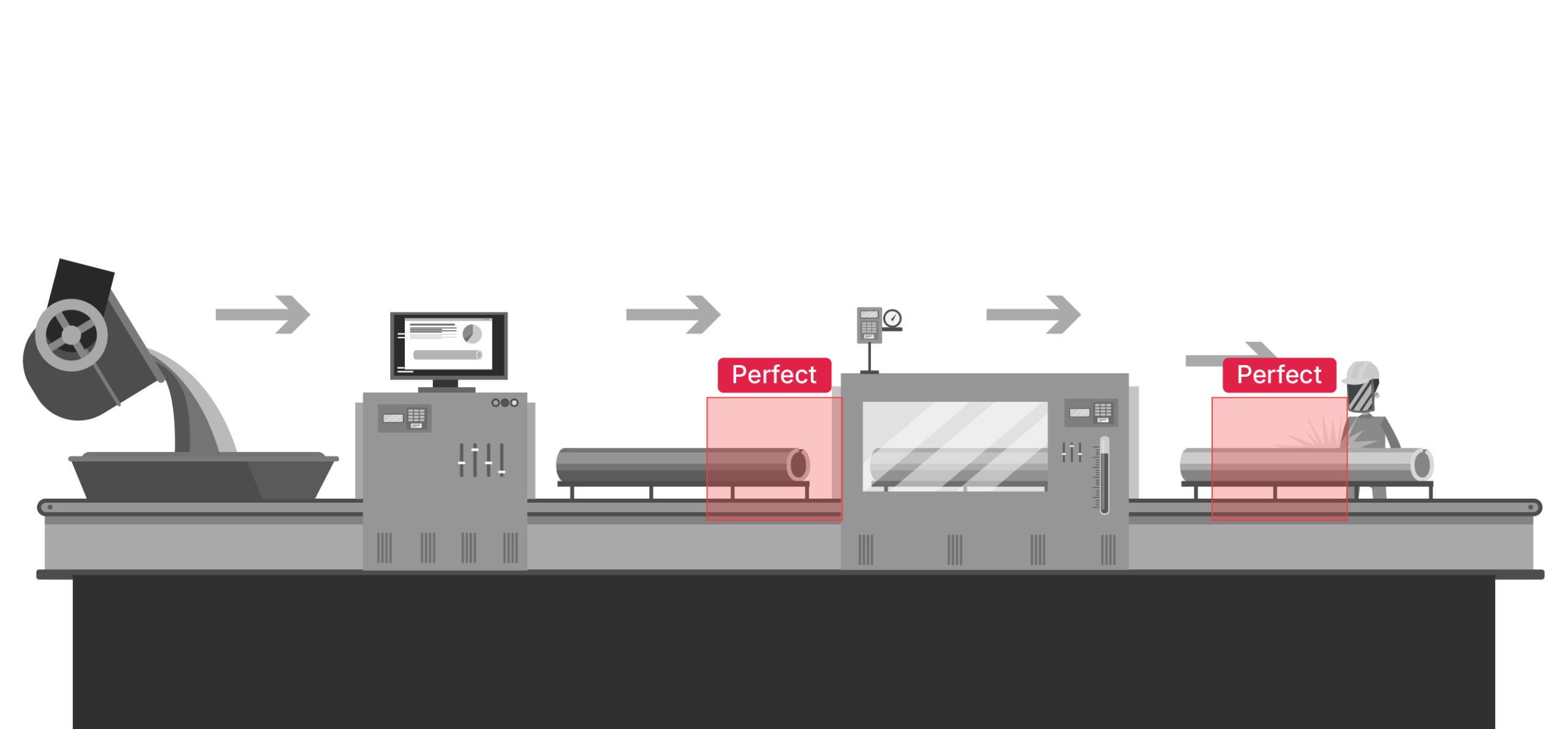
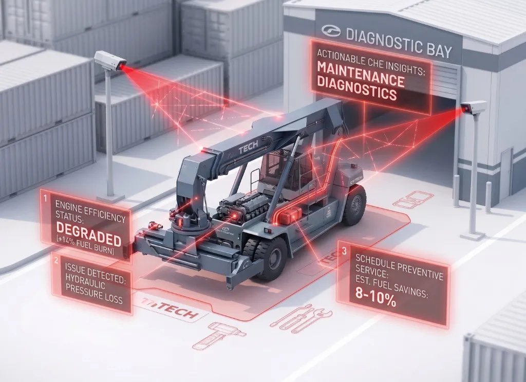
Maintenance is equally important. Equipment that is not properly maintained tends to consume more fuel. Issues such as engine inefficiency, hydraulic problems, or tyre wear can significantly increase fuel consumption without being immediately visible.
By shifting focus from just container flow to equipment behavior, yard operators gain a more accurate understanding of where fuel is being spent, and wasted.
Actionable CHE Insights
Data becomes valuable only when it leads to action. Simply knowing where equipment is located is not enough; the real benefit comes from using that information to make smarter operational decisions.
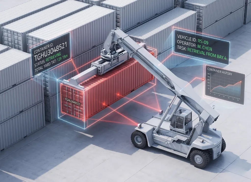
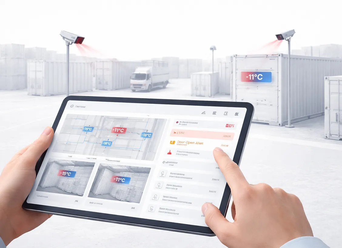
Geo-location tracking of CHE provides real-time visibility into equipment movement. Yard managers can see which machines are active, which are idle, and how they are being utilized across different zones. This allows for dynamic task allocation, where the nearest available equipment is assigned to a job, reducing travel distance and fuel usage.
Active status monitoring adds another layer of insight. By tracking whether equipment is actively working, idling, or inactive, operators can identify patterns of inefficiency. For example, if certain machines spend excessive time idling during specific shifts, it may indicate scheduling gaps or coordination issues.
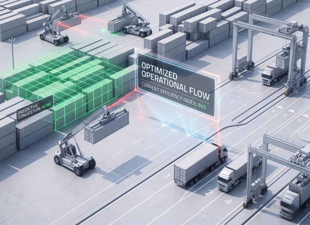
Routing optimization becomes significantly more effective with these insights. Instead of relying on fixed movement patterns, routes can be adjusted based on real-time conditions within the yard. Congested areas can be avoided, and equipment can be directed along the most efficient paths.
These improvements may seem incremental, but their cumulative impact is substantial. Fewer unnecessary trips, reduced idle time, and better equipment allocation all contribute to lower fuel consumption.
Additionally, monitoring equipment usage helps in planning preventive maintenance. Machines that show irregular fuel consumption or unusual activity patterns can be flagged early, preventing costly breakdowns and further inefficiencies.
Turning Insight into Savings
When CHE insights are consistently applied, the results become measurable.
Fuel consumption begins to stabilize as unnecessary movement is reduced. Idle time decreases as equipment is better coordinated. Maintenance costs drop due to early issue detection and more balanced equipment usage.
In most optimized yards, these changes translate into a 15-20% reduction in fuel and maintenance costs. This is not achieved through drastic operational changes, but through steady improvements in visibility and decision-making.
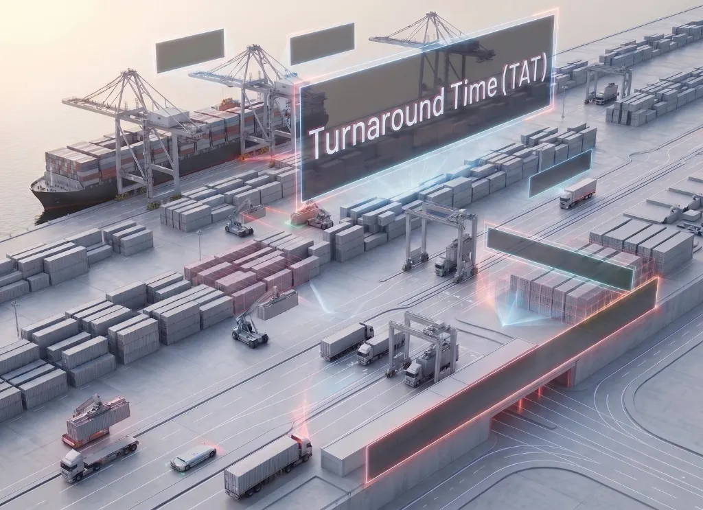
Beyond direct cost savings, there are additional benefits. Equipment lifespan improves due to reduced strain and balanced usage. Operational flow becomes smoother, leading to faster turnaround times. Teams spend less time dealing with inefficiencies and more time executing planned tasks.
From a financial perspective, the return on investment is clear. Lower fuel expenses, reduced maintenance costs, and improved productivity contribute directly to higher margins.
Moving Forward
Fuel efficiency in container yards is not about restricting usage; it is about making every movement count. When equipment operates with purpose and coordination, fuel consumption aligns naturally with productivity.
The key lies in visibility and control. By tracking CHE location, monitoring active status, and applying data-driven insights, yard operators can turn one of their largest expenses into a manageable and reducible cost.
Stop letting hidden operational losses drain your profits. The Gotilo Container solution turns your biggest yard bottlenecks into your strongest assets.
