WebOccult Insider | Nov 25

When Insight Finds Immediacy

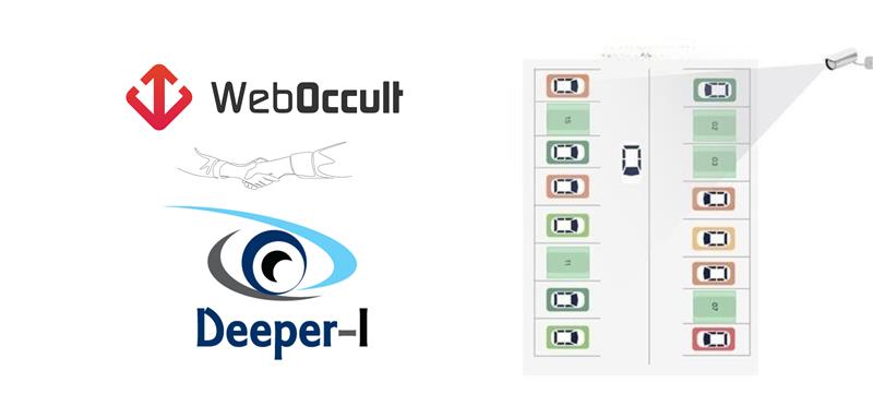
WebOccult + Deeper-i at Japan IT Week 2025

Collaboration is often described as two entities working together, but at Japan IT Week 2025, WebOccult and Deeper-i proved it is something much more profound: it is the convergence of seeing and doing.

This month, we are proud to spotlight our successful co-exhibition at Makuhari Messe, where we unveiled a partnership defined not just by technology, but by a shared philosophy, that intelligence should live closer to the world it serves.

The Demo
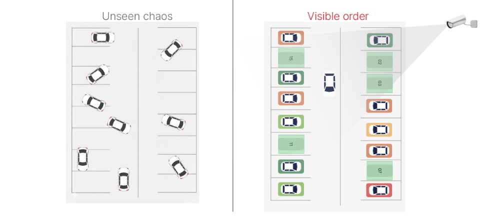
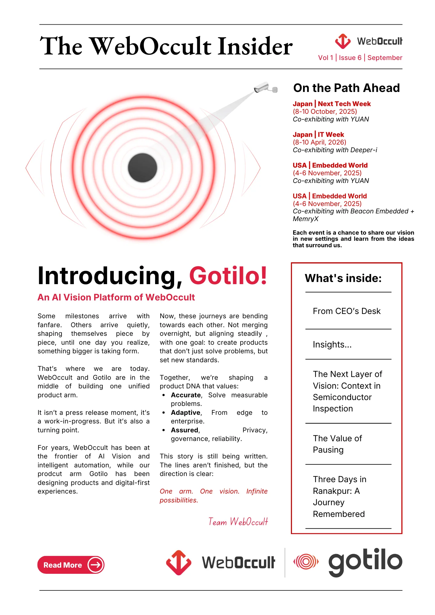
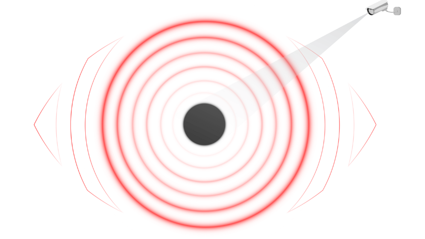
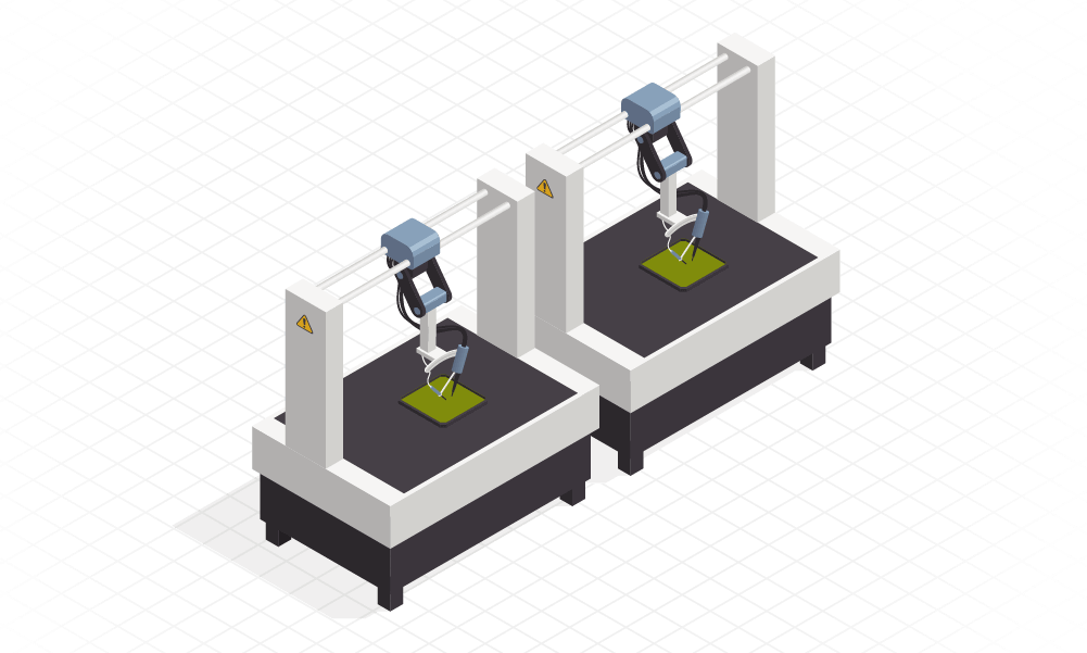
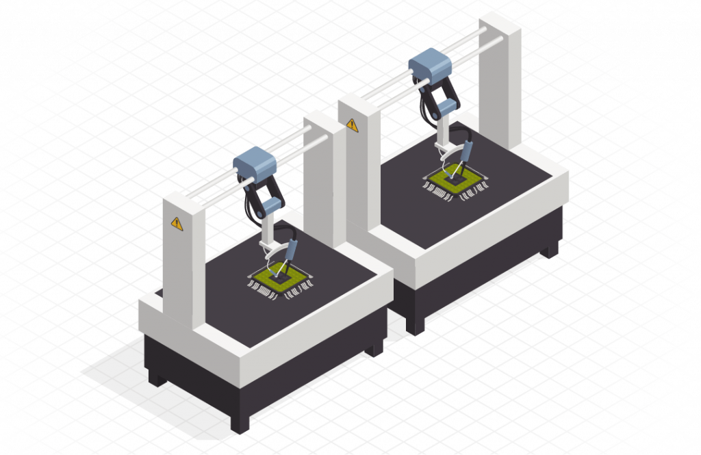
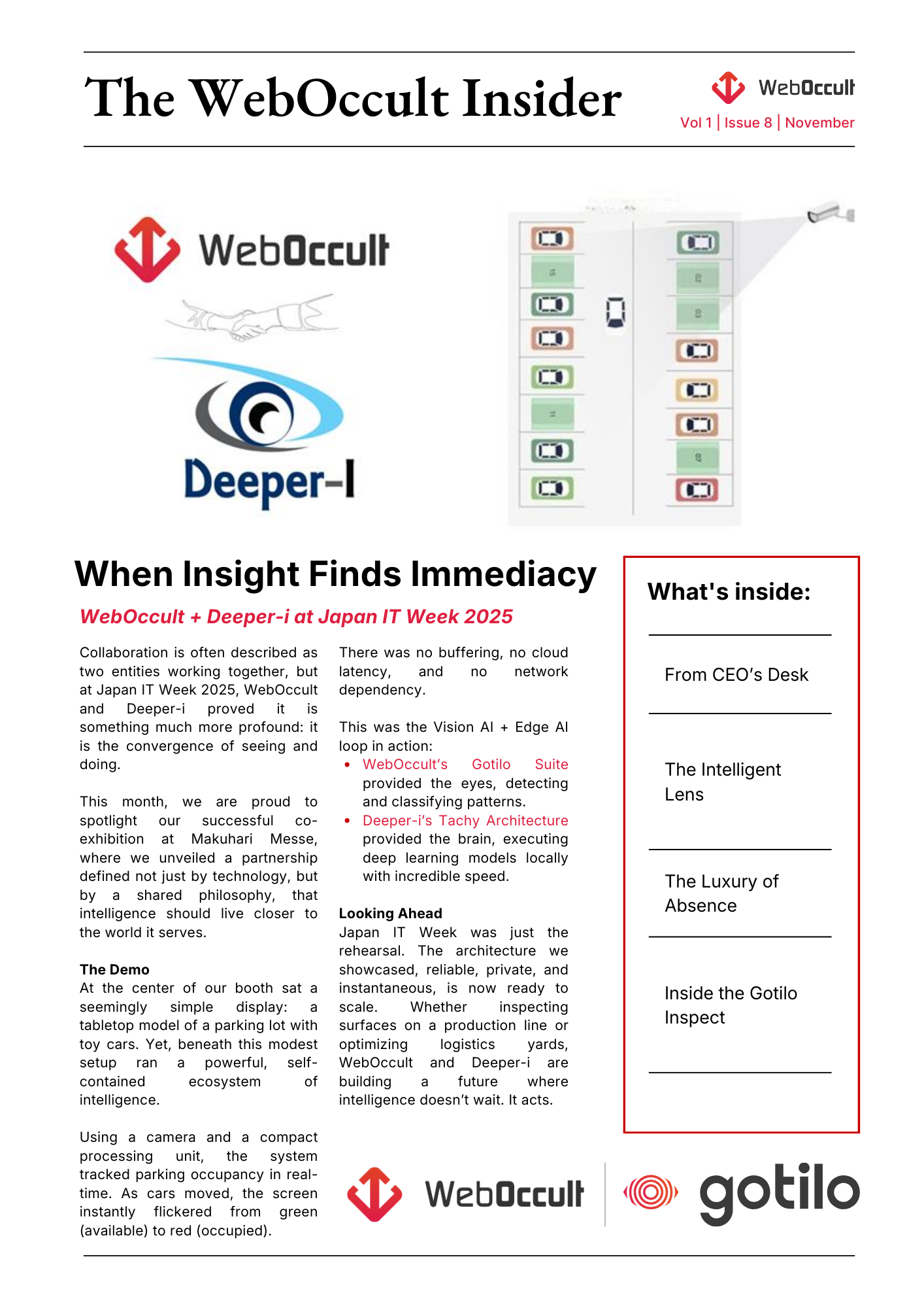
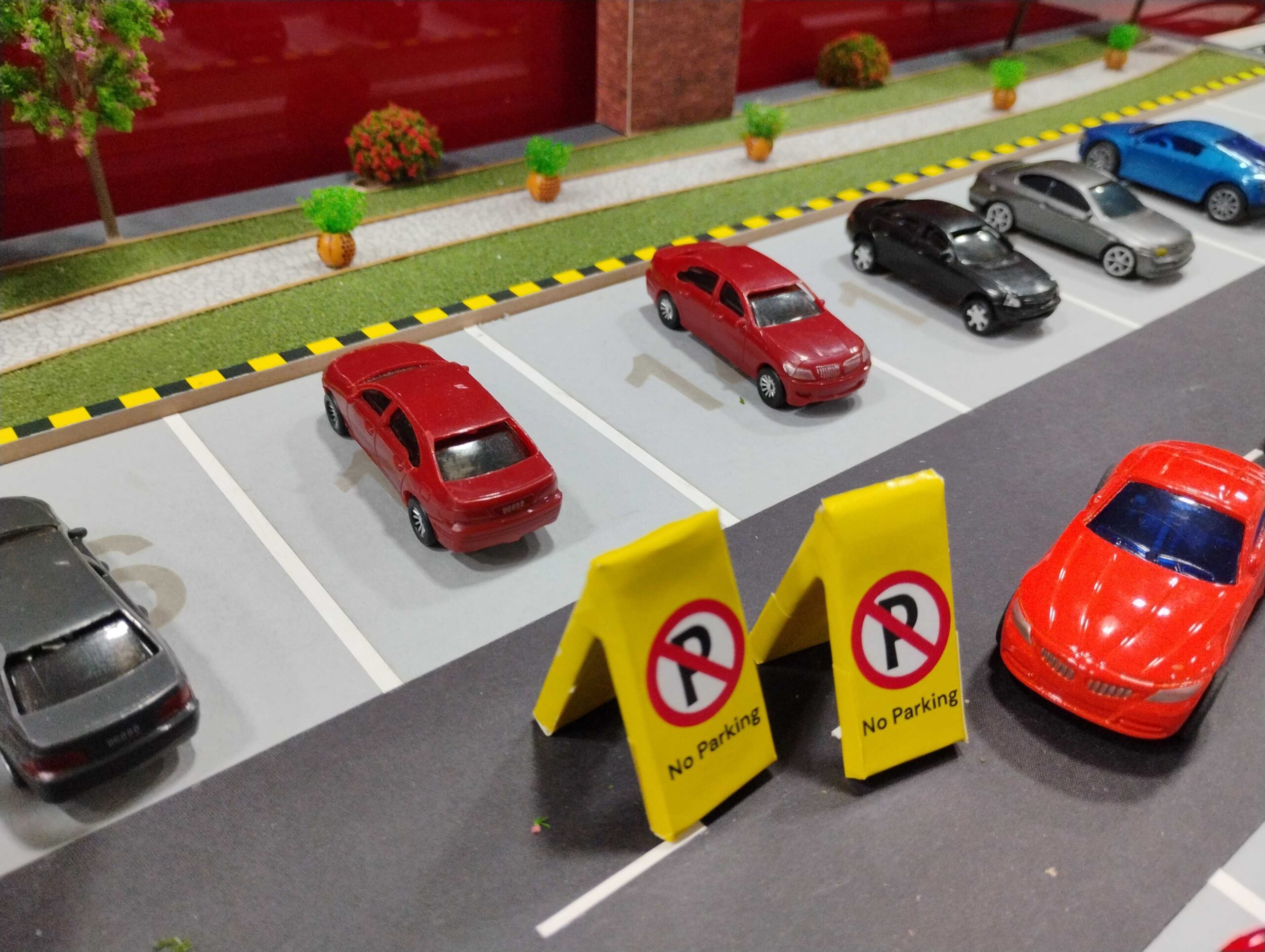
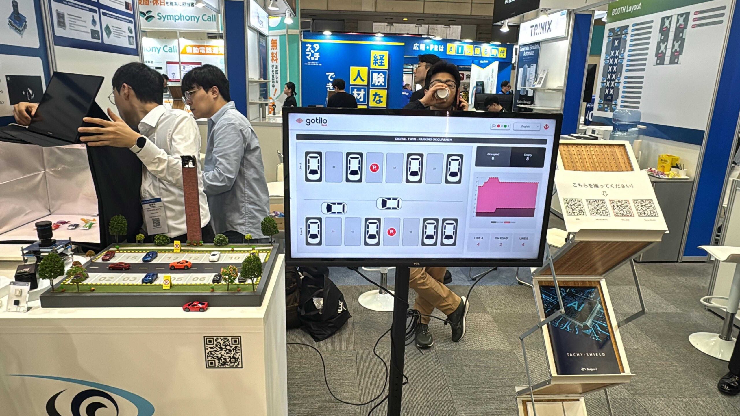
At the center of our booth sat a seemingly simple display: a tabletop model of a parking lot with toy cars. Yet, beneath this modest setup ran a powerful, self-contained ecosystem of intelligence.

Using a camera and a compact processing unit, the system tracked parking occupancy in real-time. As cars moved, the screen instantly flickered from green (available) to red (occupied).

There was no buffering, no cloud latency, and no network dependency.

This was the Vision AI + Edge AI loop in action:

  • WebOccult’s Gotilo Suite provided the eyes, detecting and classifying patterns.
  • Deeper-i’s Tachy Architecture provided the brain, executing deep learning models locally with incredible speed.

Looking Ahead

Japan IT Week was just the rehearsal. The architecture we showcased, reliable, private, and instantaneous, is now ready to scale. Whether inspecting surfaces on a production line or optimizing logistics yards, WebOccult and Deeper-i are building a future where intelligence doesn’t wait. It acts.


Simply being normal is the new normal

Do you ever feel like you’re running a marathon at a sprint pace? We are conditioned to believe that momentum is everything. We fly across oceans, we chase the next big contract, and we convince ourselves that stopping is failure.

I was recently in that exact mode. I was halfway across the world, in the middle of a major exhibition in US, surrounded by opportunity. The energy was high. The schedule was packed. I felt unstoppable. And then, in a single second, everything stopped.

Life has a funny way of reminding you who is really in charge. A sudden breakage. An unexpected physical limitation. Just like that, the meetings didn’t matter. The strategy didn’t matter. The only thing that mattered was getting home. I had to leave everything behind and make an urgent U-turn. When you are forced to hit the brakes that hard, it feels like a sacrifice. You sit there thinking about the what ifs. You worry about the momentum you’re losing. You feel like you are letting people down.

But as I sat at home over the last few weeks, forced to slow down, my perspective shifted. We spend so much time trying to optimize our lives for growth. We want 10x revenue. We want faster deployments. We want maximum efficiency. But we rarely optimize for maintenance. We’ve heard the term ‘The New Normal’ a million times since 2020. Usually, it refers to remote work or AI adoption.

But for me? I have a different definition now. To simply be normal is the ultimate luxury. Getting back to my routine didn’t feel like a chore; it felt like a gift. Returning to Square One wasn’t a regression. It was a relief. When you experience a breakage, you realize that the baseline, the simple act of being functional, is actually the foundation of everything else. You can’t build a skyscraper if the ground beneath you is shaking.

You don’t need to wait for a breakage to appreciate the routine. Don’t resent the mundane parts of your day. Don’t be so obsessed with the next milestone that you ignore the health and stability that allows you to chase it in the first place.

I’m back at my desk now. I’m back to the grind. But I’m doing it with a little more gratitude for the boring, normal, beautiful routine.

Sometimes, the biggest win is simply having the strength to stand still.


The Intelligent Lens

Why AI is Finally Making Sense of the World

If you look back at how we used technology just a year ago, it feels like a different era because the speed of innovation in 2025 has been absolutely relentless. We used to think of cameras as just digital eyes that passively recorded whatever happened in front of them, but as we close out this year, that definition has completely shifted. The biggest breakthrough this season isn’t just about spotting a car or a person, but understanding the story behind what they are doing.

We are finally moving away from systems that just draw simple boxes around objects and entering a phase where we can actually talk to our cameras. Imagine being able to ask a security feed a plain English question like ‘Is the forklift blocking the emergency exit?’ and getting an immediate, intelligent answer without a human ever needing to look at a monitor. This ability to reason and understand context means that our software is becoming less like a tool and more like an active team member that is always watching out for safety and efficiency.

Another incredible shift we are seeing right now is the ability for standard, inexpensive webcams to understand depth and distance just as well as the human eye. We no longer need expensive laser sensors or complex hardware to measure the size of a package or the distance between vehicles because the new software can figure it all out from a simple flat image. It feels like we are finally moving from a world where computers just watch to a world where they truly understand, and for us at WebOccult, that opens up a universe of possibilities for 2026.


Offbeat Essence – The Luxury of Absence

True intelligence is no longer about how much a machine says, but how intuitively it understands without saying a word.

For a decade, we built technology that begged for attention. We measured innovation by the noise it made, buzzing pockets, flashing screens, and constant alerts.

But as we close 2025, the wind is shifting. The next era isn’t about connection; it’s about anticipation.

We are entering the age of Invisible Intelligence.

True sophistication is no longer about a machine that chats with you, but one that understands you without saying a word. It is the difference between a tool that demands supervision and a partner that quietly clears the path.

The future won’t be defined by the technology you stare at, but by the technology you don’t even notice is there.


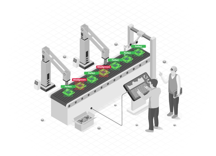
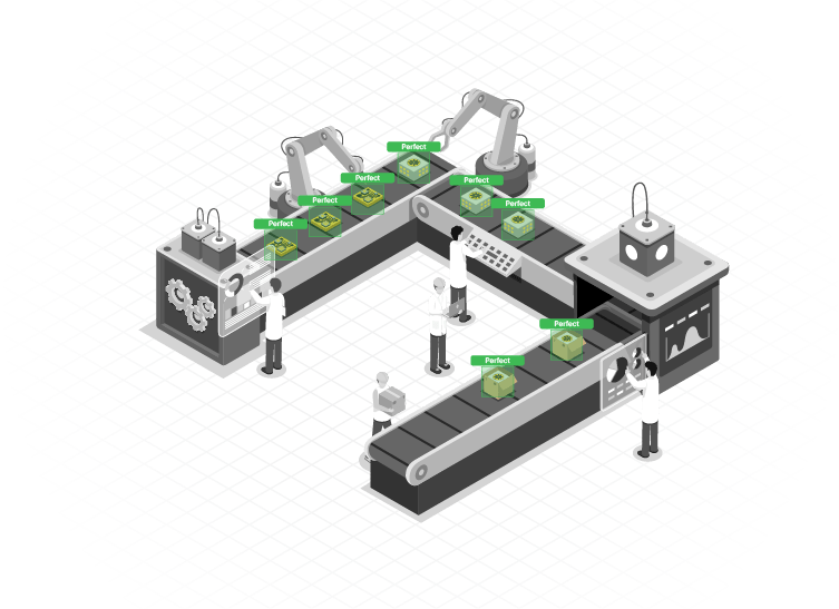
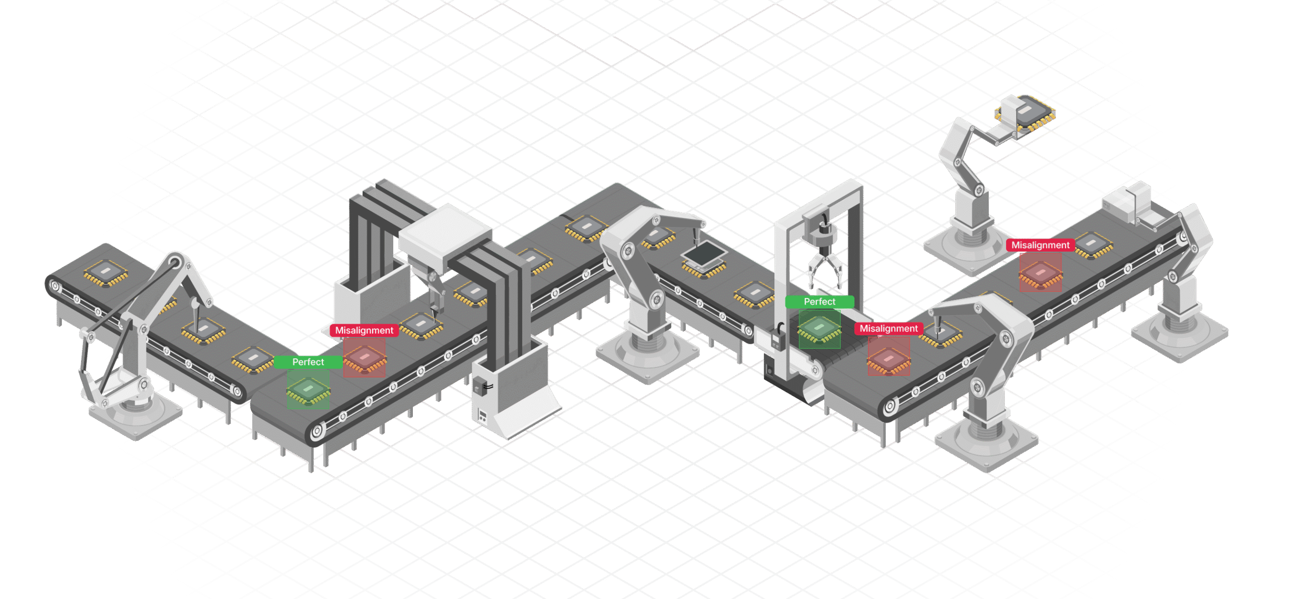
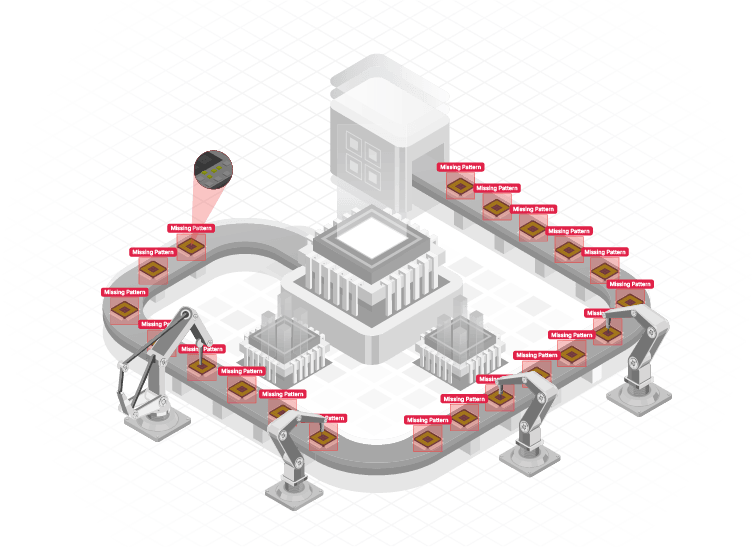
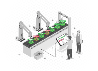
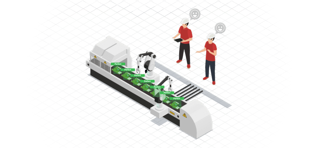
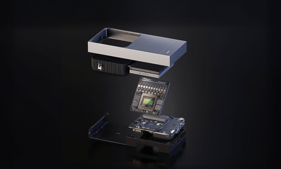
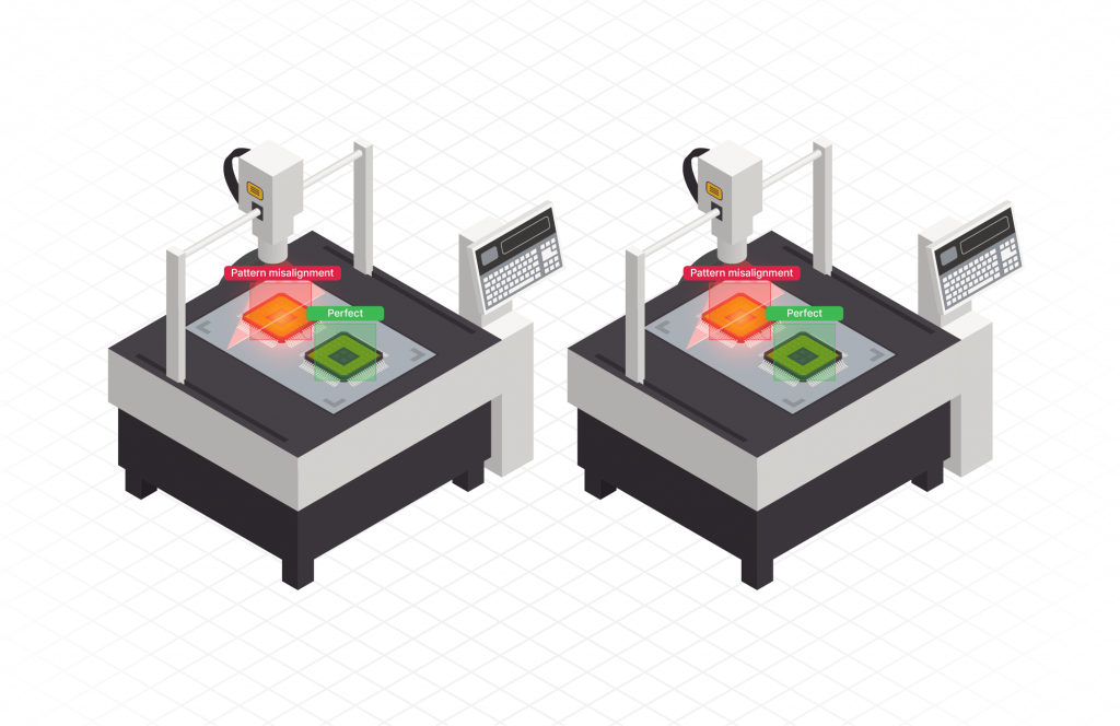
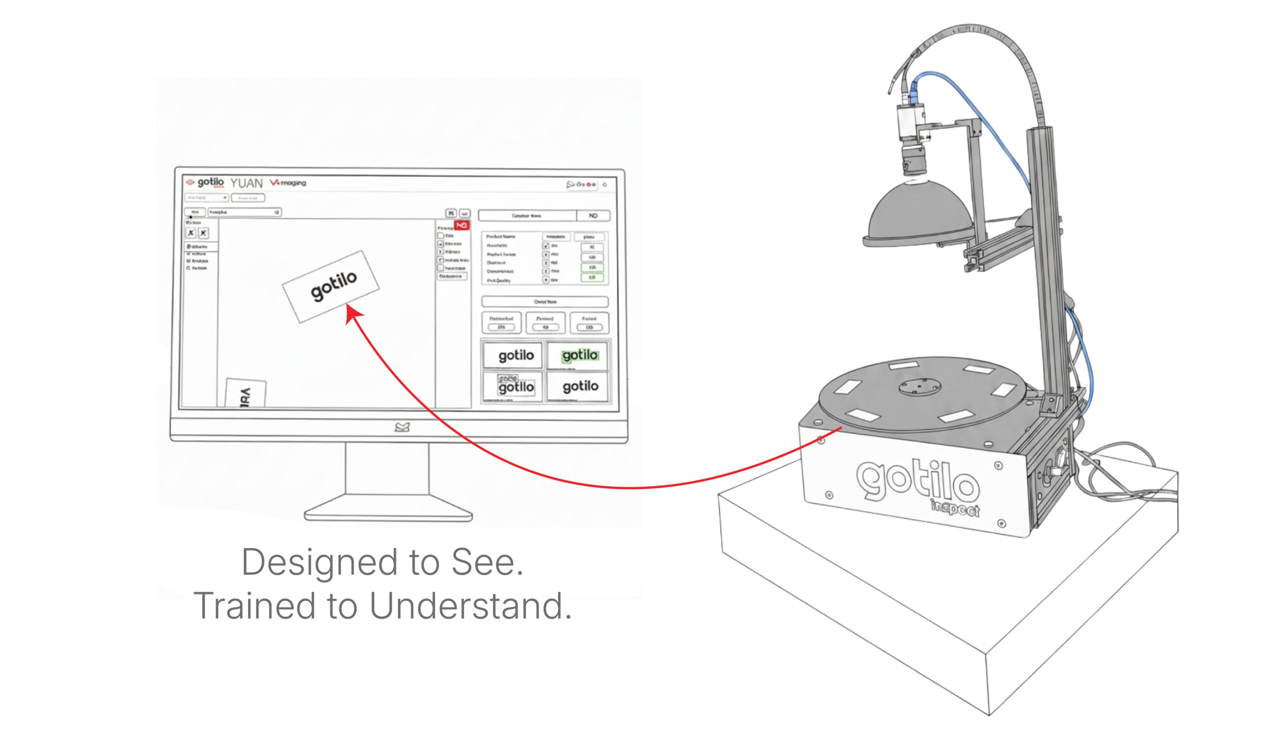
Inside the Gotilo Inspect

In the US market, the conversation around manufacturing and logistics has shifted. We are no longer just talking about automation, we are talking about operational resilience. With labor costs rising and quality standards becoming stricter than ever, American businesses can’t afford downtime, and they certainly can’t afford defects.
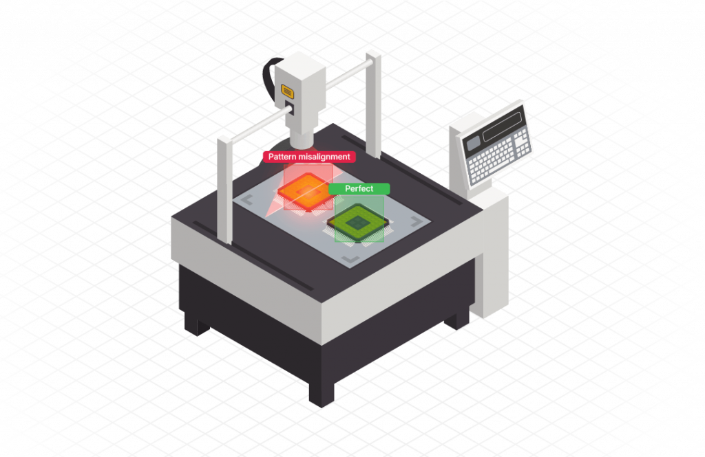
This is where Gotilo Inspect enters the equation.

I’ve spent the last few months speaking with facility managers across the States, and the pain point is universal: How do we maintain 100% quality without slowing down the line?

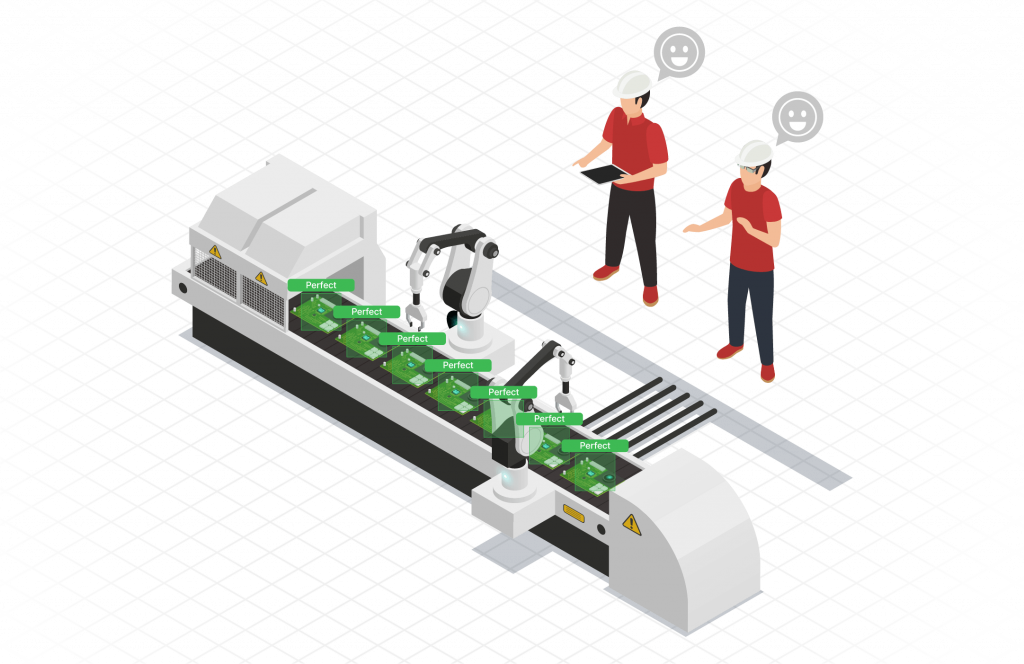
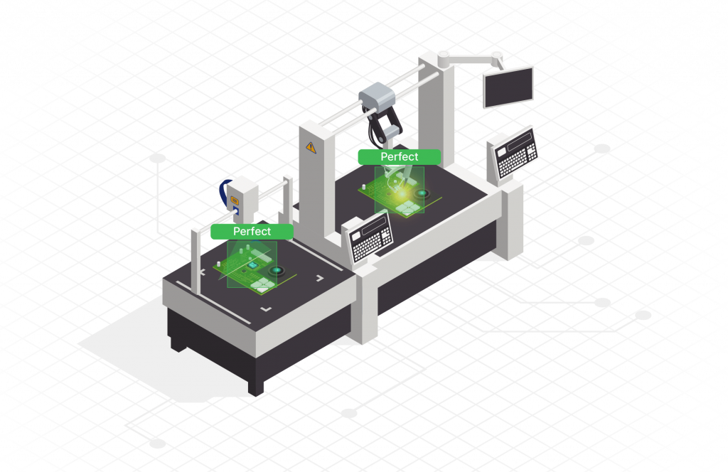
Gotilo Inspect is our answer. It is an AI-powered Visual Inspection system designed not to replace human oversight, but to give it superpowers.

Here is why it’s gaining traction in the US right now:

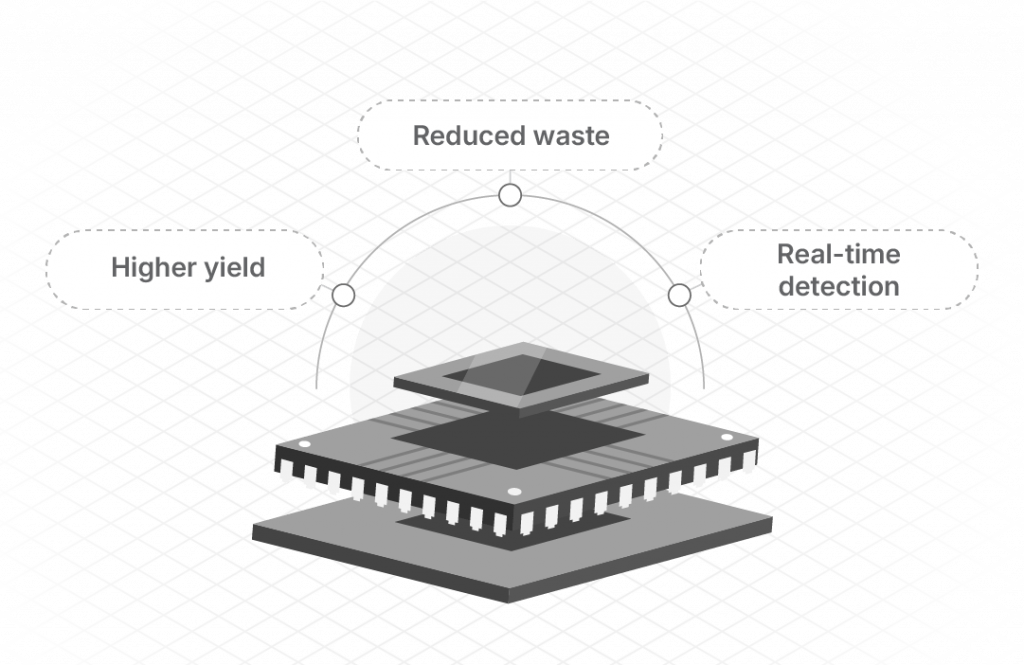
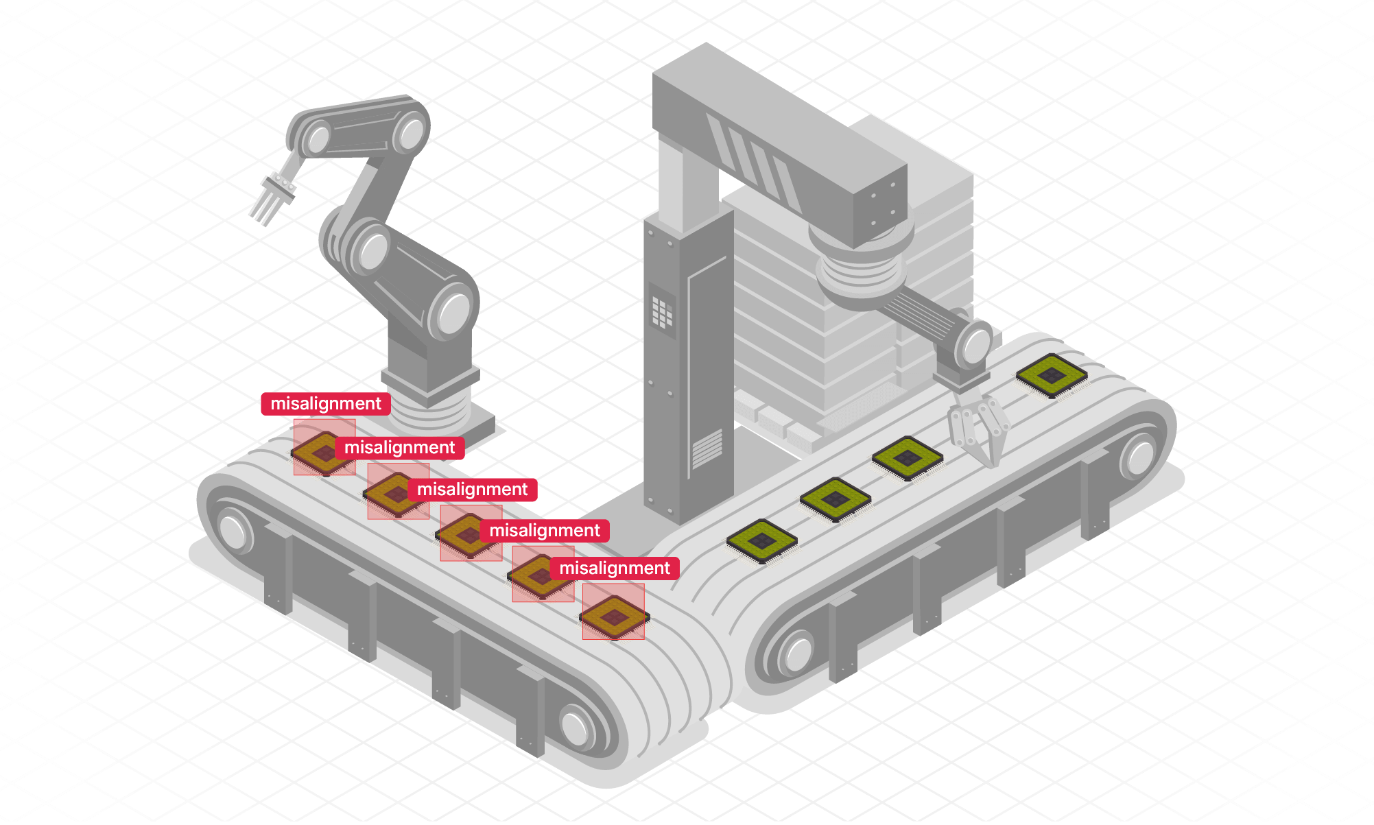
1. The End of the Random Sample

Traditional QC relies on checking every 10th or 100th unit. Gotilo Inspect offers 100% visibility. Whether it’s detecting surface scratches on automotive parts or verifying label placement on consumer goods, our algorithms check every single unit in real-time. We catch the defects that human fatigue misses.

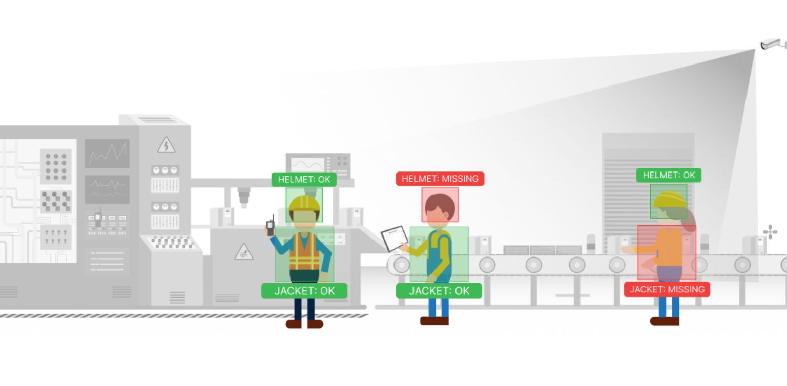
2. Safety as a Constant, Not a Checklist

In the US, liability and OSHA compliance are massive concerns. Gotilo Inspect includes robust PPE Detection and Zone Monitoring. It instantly flags if a worker enters a hazardous area without a hard hat or vest. It turns safety from a reactive policy into a proactive, always-on shield.

3. Data Privacy & Edge Execution

US clients are rightly protective of their data. Because Gotilo Inspect is optimized for Edge AI (running locally on your hardware), your proprietary production data doesn’t need to leave the building. It’s fast, secure, and bandwidth-efficient.

We aren’t just selling solution; we are selling the peace of mind that comes with knowing your facility sees everything, every time.

At the Edge of Vision – The Story of WebOccult + Deeper-I at Japan IT Week 2025

Collaboration creates a story. Some are born from timing, others from shared ambition.

But the partnership between WebOccult and Deeper-I began from something subtler, a mutual belief that intelligence should live closer to the world it serves.

For years, Vision AI has been mastering the art of seeing, while Edge AI has been perfecting the act of doing. When these two disciplines finally converge, something remarkable happens: insight finds immediacy. 

At Japan IT Week 2025, that convergence came to life in a small, living demonstration, a model of a parking lot no bigger than a tabletop, where cars were not only seen but understood in real time.

At first glance, the booth display seemed simple. Toy cars arranged in a miniature parking grid, a compact camera hovering overhead, a screen alive with flickering boxes of color, green for available, red for occupied. Yet beneath this understated setup existed a complete, self-contained ecosystem of intelligence.

The demonstration represented the full cycle of Vision AI meeting Edge AI: from frame capture to inference, from decision to visualization, all without a single trip to the cloud.

It was intelligence happening exactly where the world moved.

The Collaboration

The partnership between WebOccult and Deeper-I is defined by complementarity. WebOccult, with its Gotilo Suite, brings deep expertise in image understanding, the ability to detect, classify, and interpret patterns that form meaning. Deeper-I, through its Tachy Edge AI architecture, contributes the engineering precision that makes those insights possible in real time.

The two systems together represent more than compatibility; they represent philosophy in motion, a shared conviction that clarity should not wait for connectivity, and intelligence should not depend on distance.

In this collaboration, WebOccult’s software learns from vision, while Deeper-I’s hardware learns from motion. The result is a form of intelligence that doesn’t just analyze but responds, instantly, locally, and reliably.

The Demonstration at Japan IT Week 2025

At the co-exhibition booth in Makuhari Messe, the teams showcased a real-time car parking occupancy detection system, designed entirely for edge execution.

The setup integrated several components, each working in balance. At the core was the Tachy BS402 Neural Processing Unit (NPU), Deeper-I’s accelerator dedicated to running deep learning models at the edge. Mounted atop a Tachy Shield (HAT) on a Raspberry Pi 4, it enabled high-speed SPI communication between host and accelerator. The Pi captured live frames from a USB camera, powered by a Pi 5 adapter and connected via Micro HDMI to HDMI to an external monitor for real-time output. The camera, fixed on a stable mount overlooking the parking grid, delivered a continuous feed to the Pi, each frame representing a tiny slice of reality to be read, processed, and visualized.

Visitors could see the system work before their eyes. Cars moved within the model, and the camera, through Gotilo Inspect’s AI pipeline, immediately detected the change. Bounding boxes appeared, confidence scores updated, occupancy states shifted in real time. No buffering, no delay, no network dependency. 

The intelligence lived right there, on the desk, as immediate as a human glance.

The Technical Architecture

The demonstration was more than visual magic; it was a complete Edge AI pipeline compressed into a single table. It showcased how software and hardware communicate when designed with harmony rather than hierarchy.

The backend handled inference and data processing, while the frontend provided visualization, together forming a closed loop of awareness. Each frame captured by the USB camera was first received by the Raspberry Pi, pre-processed, and sent to the Tachy NPU through SPI-based data transfer.

The NPU performed the neural inference, executing a custom YOLOv9-based detection model that had been optimized and compiled into Tachy format for compatibility with the Tachy-RT runtime. Once inference was complete, the processed tensors were transmitted back to the Pi, where Python-based post-processing handled bounding box decoding, class labeling, and confidence scoring.

This intermediate layer, subtle but essential, converted raw predictions into recognizable insight. The post-processed data was then passed through a socket-based communication layer to a Flask-built frontend dashboard, which visualized the results dynamically in a browser.

Each parking slot appeared as a color-coded rectangle, a direct reflection of the system’s perception of the miniature world beneath the lens.

The entire data flow could be summarized as:
Camera – Raspberry Pi – Tachy HAT (via SPI) – Raspberry Pi – Socket Transfer – Flask Frontend UI.

The input resolution of 480×480 pixels balanced visual clarity with computational efficiency, allowing the model to perform consistently on embedded hardware. Every element of the setup, from lighting to frame rate, was calibrated for reliability rather than spectacle.

What visitors experienced was not a simulation but a functional prototype, a distilled version of what an industrial Vision AI system looks like when it runs on its own.


Why Edge Intelligence Matters

The choice to perform inference at the edge rather than in the cloud is not merely technical, it’s philosophical. Traditional vision systems rely on distance: cameras send data to remote servers, where it is processed and returned with results. That model introduces delay, bandwidth dependency, and often, privacy concerns. In contrast, Edge AI collapses that distance. Computation occurs directly at the source, on devices capable of learning, deciding, and acting in real time.

In manufacturing, logistics, or mobility, this proximity changes everything. A second saved in processing is a fault prevented, a decision optimized, an error avoided. The collaboration between WebOccult and Deeper-I demonstrates this shift in real form: Gotilo’s interpretive algorithms providing meaning, Deeper-I’s Tachy architecture delivering immediacy. The intelligence does not travel; it stays. It learns the rhythm of its own environment.

This isn’t just efficiency, it’s empathy, designed in silicon. Systems that see and decide where the action occurs begin to feel less like tools and more like participants in the process they monitor.

Designing Systems People Can Trust

All advanced systems, no matter how elegant, are ultimately measured by trust. At the exhibition, visitors didn’t ask how many frames per second the system achieved. They asked if it could be trusted to decide correctly.

That question defines the future of AI adoption more than any technical metric.

By keeping the entire inference loop visible and local, the WebOccult + Deeper-I demonstration offered transparency as much as precision.

Visitors could trace the logic in real time, from camera capture to bounding box display, understanding not just what the system decided, but how. This transparency builds reliability, and reliability becomes trust.

In many ways, Edge AI is not only an architectural improvement, it’s an ethical one. It decentralizes not just data, but responsibility. When systems explain themselves, people believe in them. That’s how technology becomes part of the human workflow instead of sitting above it.

The Broader Impact and Future Direction

The success of this demonstration is not confined to parking occupancy. It represents a blueprint for how Vision AI and Edge AI can collaborate across industries. The same architecture can inspect surfaces in manufacturing, verify shipments in logistics yards, monitor dwell times in ports, or analyze movement in smart cities, all without dependency on cloud infrastructure.

In this future, cameras don’t just see, they understand. Machines don’t just compute, they interpret. Every industrial space, from production floors to distribution hubs, can become an ecosystem of self-reliant intelligence.

The WebOccult + Deeper-I partnership is already extending this concept into new verticals. In manufacturing, the combination of Gotilo Inspect with Tachy Edge AI will support label inspection, defect detection, and process visibility.

In logistics, the same architecture can optimize resource allocation through real-time analytics. Across these domains, the objective remains the same: to make intelligence not louder, but closer; not faster, but truer.

Building Precision That Stays

The demonstration at Japan IT Week 2025 wasn’t simply a collaboration between two companies. It was a rehearsal for a future where intelligence performs where life happens. From the small tabletop model to the embedded pipeline running beneath it, everything reflected one guiding principle: proximity creates clarity.

For WebOccult, this is the natural evolution of Gotilo’s Vision AI. For Deeper-I, it is the next chapter in Edge computing’s maturation. For industries around the world, it is a glimpse of how technology can become truly dependable, not by existing everywhere, but by existing exactly where it’s needed.

At the edge, intelligence doesn’t wait. It acts. And in that instant, vision becomes understanding.

Want a closer look at how the parking demonstration was engineered? Read our detailed breakdown in The Technical Anatomy of a Parking Twin

To explore how Vision AI and Edge AI can transform your industry’s visibility and precision, visit www.weboccult.com or connect with our team to experience the future of inspection!

The Intelligence of Reading – How Vision AI Learns to Understand Surfaces

Any object that leaves a factory belt carries an identity. It may appear as a string of numbers etched into metal, a barcode printed on paper, or a label attached to packaging or glass material.

Together, these small symbols form the nervous system of modern industry. They track movement, record responsibility, and ensure that everything built, moved, or sold remains connected to its source.

But these identifiers are only as reliable as the eyes that read them.

For years, humans have performed that task with patience and discipline, verifying serial numbers, expiry dates, and labels under harsh light and long shifts. Yet even the most diligent eyes grow tired. Even the clearest labels fade.

The arrival of Vision AI has given this everyday process a new kind of precision, one that reads, verifies, and understands not just what is written, but what is meant.

This is the story of how machines learned to read the world with accuracy, and how that ability is reshaping the way industries see themselves.

The Hidden Language of Surfaces

Every plate and label is a fragment of communication.A serial number stamped on steel tells where a component was made. A barcode links a shipment to its destination. An expiry label defines a product’s safety. These markings translate the invisible flow of supply chains into a physical form that can be verified, tracked, and trusted.

The challenge has always been consistency. Ink fades. Surfaces deform. Machines print imperfectly.

In these imperfections lie the need for a technology that can observe, interpret, and correct in real time. Vision AI does not simply detect these identifiers; it reads them.

Each image captured is transformed into a structured understanding, text recognized, imperfections mapped, context verified. What once required manual checks across hundreds of units can now be observed with the precision of thousands of simultaneous, tireless eyes. This shift, from sight to understanding, defines the new era of inspection.

Why Reading Matters

In industrial environments, reading is accountability. The act of recognition connects an item to its origin and ensures it reaches its intended destination without error.

When that reading fails, even once, the impact ripples outward: a mislabeled shipment disrupts inventory; an unreadable code delays logistics; an unverified batch compromises safety compliance.

Across manufacturing, logistics, and packaging, every character matters. It’s not just about visibility, it’s about truth in operation.

Manual verification is slow, inconsistent, and expensive. Traditional optical character recognition (OCR) systems, while useful, often struggle with variable lighting, skewed angles, or worn surfaces. They see, but they don’t adapt. Vision AI addresses this gap by introducing adaptability, a form of intelligence that doesn’t extract symbols but interprets conditions.

It reads the way humans do, in context, not isolation. Where the human eye grows tired, the system grows more confident. Where environments change, it recalibrates.

The Complexity Behind Clarity

The act of reading seems simple, until you ask a machine to do it flawlessly.

Every plate or label introduces its own challenges:

  • Glare and reflection from polished surfaces distort character edges.
  • Irregular materials like brushed metal or textured plastics affect contrast.
  • Varying fonts, print sizes, and languages complicate pattern recognition.
  • Motion blur on high-speed production lines makes steady focus difficult.
  • Environmental factors like heat, dust, or humidity introduce unpredictable variation.

These details may seem minor, yet they define the reliability of automation. A single misread plate can invalidate entire production batches or delay shipment verification.

Solving these problems requires systems that understand not just what they see, but how they’re seeing it. Vision AI provides that understanding by analyzing the surface, light, and structure of each image, teaching the model to recognize not just characters, but the conditions under which those characters exist.

The result is not perfect images, but perfect understanding.

Vision AI as an Interpreter

Traditional OCR reads what is present. Vision AI reads what is possible. This distinction is subtle, but transformative.

A conventional OCR engine identifies patterns of pixels and matches them to known characters. A Vision AI-based system does this too, but with additional layers of interpretation:

  • It learns texture.
  • It distinguishes noise from signal.
  • It recognizes when a character is missing, distorted, or overlapped, and predicts its meaning based on context.

This is not guessing. It is learning through precision. Deep neural networks trained on diverse datasets, including poor lighting, angled views, and damaged labels, allow the system to see more clearly under real conditions.

By combining defect detection, pattern matching, and OCR within a single framework, Vision AI transforms inspection from a linear task into a cognitive process.

Recognition is no longer mechanical. It becomes interpretive, a quiet form of understanding where context gives meaning to data.

The Technical Architecture of Plate & Label Inspection

Behind every moment of understanding lies a sequence of design. The technical anatomy of plate and label inspection can be viewed as six interconnected layers:

  • Image Acquisition: High-resolution cameras capture the surface under controlled or adaptive lighting. The aim is not perfect imagery but sufficient clarity for consistent interpretation.
  • Preprocessing: Algorithms normalize lighting, correct distortions, and filter background noise.The system adjusts dynamically to surface reflectivity and motion.
  • Detection: Deep learning models locate the region of interest, isolating plates or label areas for focused analysis.
  • OCR & Defect Recognition: The system identifies and extracts alphanumeric characters while detecting surface defects such as print misalignment, faded ink, or scratches.
  • Validation: Extracted data is cross-verified against stored templates, expected formats, or reference datasets. Each reading carries a confidence score, ensuring traceability.
  • Visualization & Output: Results appear on dashboards or integrate with enterprise systems. Operators view live results, accuracy metrics, and system health, all in real time.

Each layer acts as an independent lens. Together, they produce comprehension.

Design Philosophy: Reading as Precision

The essence of this technology lies not only in what it sees, but in how it decides to see. Vision AI engineers talk about accuracy in decimals. Designers, however, talk about empathy, about creating systems that interpret rather than assume.

In plate and label inspection, that empathy becomes precision. Every millisecond, the system must balance speed and certainty, ensuring that throughput never compromises truth. Designing for precision means designing for restraint, teaching the model to know when to trust, when to recheck, and when to ask for human validation.

This is what distinguishes understanding from automation. A system that reads every character perfectly but fails to question an anomaly is efficient, but not intelligent. True intelligence holds space for uncertainty, for the slight pause that ensures accuracy.

From Inspection to Insight

Reading is only the beginning. Once information is captured, it becomes part of a much larger structure, the continuous feedback loop of industrial intelligence.

  • Manufacturing: Vision AI verifies serial plates and lot codes to ensure quality and traceability across production stages.
  • Logistics: Real-time label validation prevents misrouting, reduces warehouse errors, and improves traceability.
  • Automotive: VIN plate inspection and surface engraving validation ensure identity integrity for safety and compliance.Automotive: VIN plate inspection and surface engraving validation ensure identity integrity for safety and compliance.
  • Pharma & Packaging: Expiry date OCR and label defect detection maintain regulatory standards.
  • FMCG & Retail: Ensures label uniformity, print quality, and brand consistency across high-volume packaging lines.

Each of these applications contributes to a larger shift, from reaction to anticipation. Industries no longer wait for errors to appear; they monitor patterns and prevent them before they occur.

Inspection becomes awareness. Awareness becomes intelligence.Intelligence becomes value.

The Future of Reading

The next generation of plate and label inspection will move beyond simple OCR. It will read context, understanding that a missing digit in a part number carries a different consequence than one in a shipping label.

Future systems will:

  • Integrate semantic reasoning, understanding what each symbol means within its operational context.
  • Learn environmental adaptation, optimizing exposure and focus automatically under changing factory conditions.
  • Collaborate with robotics, allowing autonomous arms to act based on verified identification.
  • Employ predictive correction, suggesting likely character replacements based on historical accuracy data.

Eventually, reading itself will no longer be the task, interpretation will be. And interpretation will define the standard of precision. Machines will understand its purpose.

The Human Element

Even the most advanced system is still built upon human curiosity. Behind every accurate readout stands an engineer who once asked, “What if a machine could notice the same imperfections we do?”

Vision AI continues that tradition of observation, extending the reach of human attention rather than replacing it. When machines learn to see as we do, they remind us why we looked in the first place: to understand, to connect, to ensure that what we build reflects our intent.

In the end, every verified label is a small act of trust, between design and delivery, between people and the systems that serve them.

Trust, after all, is the most precise measurement of all.

At WebOccult, we design vision systems that don’t just watch, they interpret. Our Gotilo Inspect solution brings this capability to life through advanced plate and label inspection powered by Vision AI.

It identifies, inspects, and interprets, reading alphanumeric patterns, detecting imperfections, and verifying every plate with measurable precision. Built for real-time operation, it performs directly at the edge, transforming inspection from a routine process into a self-sustaining system of understanding.

From manufacturing floors to logistics networks, Gotilo Inspect ensures that every symbol, mark, or code tells its story accurately, the first time, every time.

Because true intelligence learns to understand.

Discover Gotilo Inspect and its applications in precision inspection at www.weboccult.com

WebOccult Insider | Oct 25

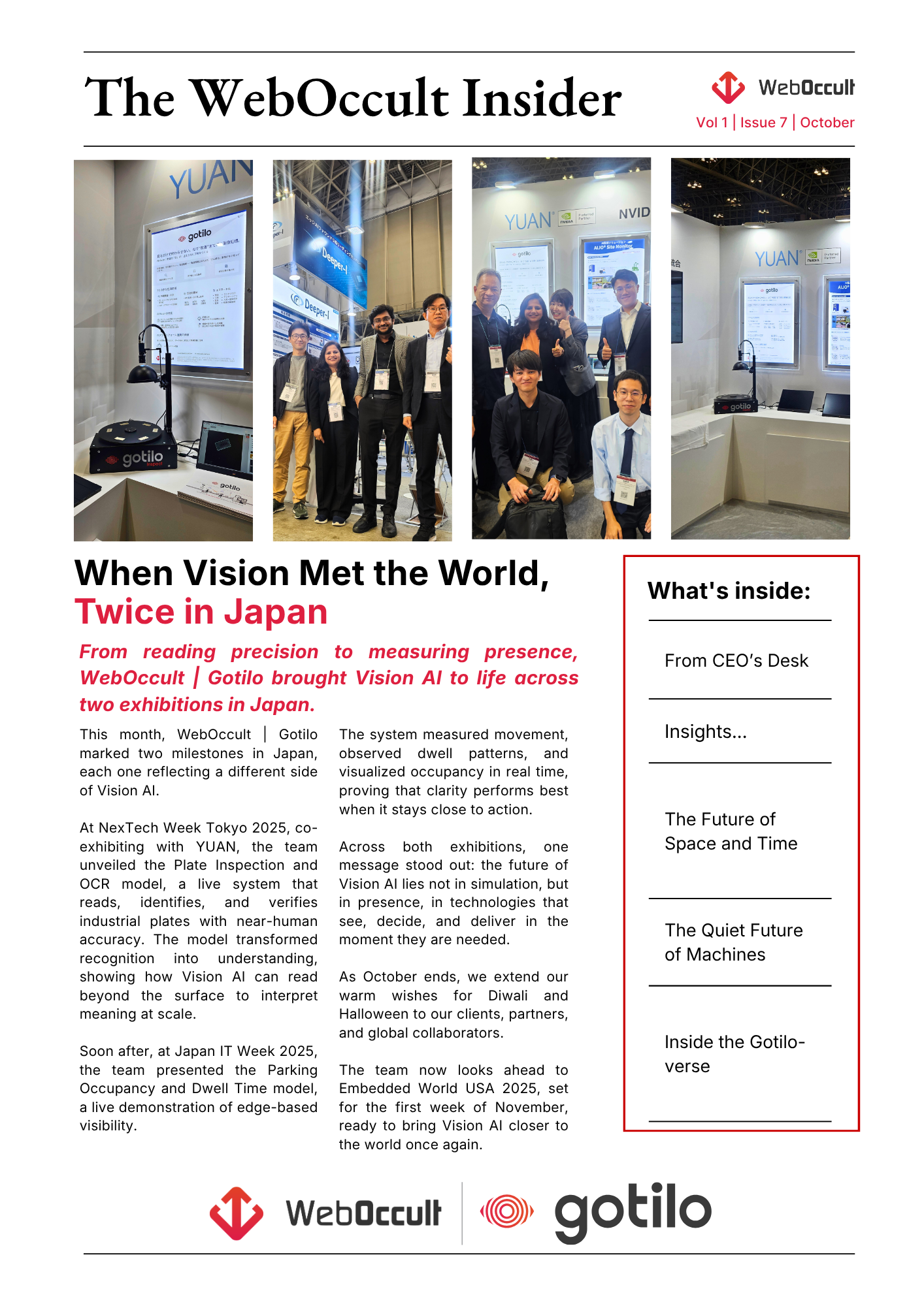
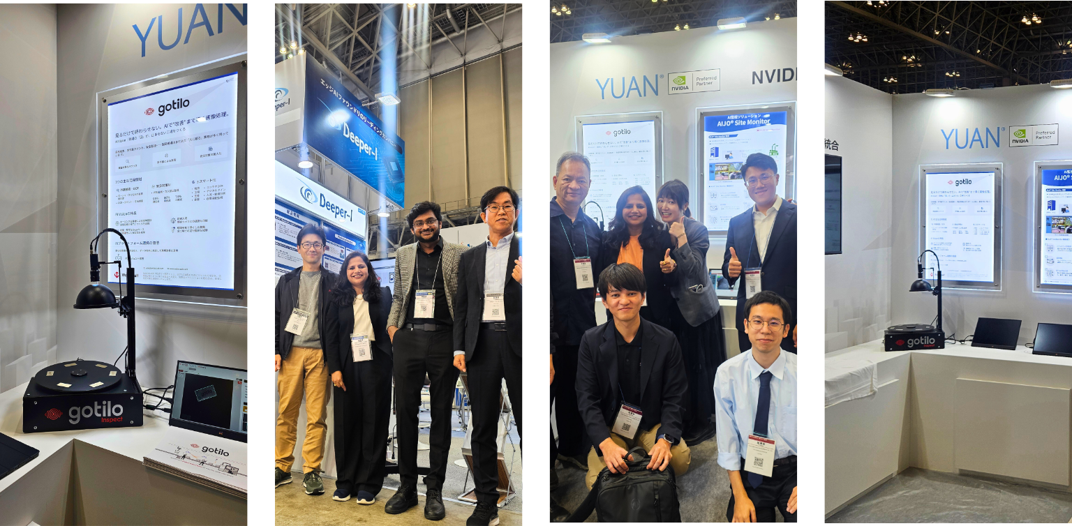
When Vision Met the World, Twice in Japan

From reading precision to measuring presence, WebOccult | Gotilo brought Vision AI to life across two exhibitions in Japan.

This month, WebOccult | Gotilo marked two milestones in Japan, each one reflecting a different side of Vision AI.

At NexTech Week Tokyo 2025, co-exhibiting with YUAN, the team unveiled the Plate Inspection and OCR model, a live system that reads, identifies, and verifies industrial plates with near-human accuracy. The model transformed recognition into understanding, showing how Vision AI can read beyond the surface to interpret meaning at scale.

Soon after, at Japan IT Week 2025, the team presented the Parking Occupancy and Dwell Time model, a live demonstration of edge-based visibility.

The system measured movement, observed dwell patterns, and visualized occupancy in real time, proving that clarity performs best when it stays close to action.

Across both exhibitions, one message stood out: the future of Vision AI lies not in simulation, but in presence, in technologies that see, decide, and deliver in the moment they are needed.

As October ends, we extend our warm wishes for Diwali and Halloween to our clients, partners, and global collaborators.

The team now looks ahead to Embedded World USA 2025, set for the first week of November, ready to bring Vision AI closer to the world once again.

On exhibitions, encounters, and the rhythm of progress!

There is something rare about standing beside a system you’ve built and watching it work, not in a controlled lab, but in the world it was meant for.

That feeling returned twice this month, both times in Japan.

At NexTech Week Tokyo, we stood among people who saw the Gotilo Inspect Plate Inspection and OCR model in action, a camera that doesn’t just capture light, but learns to read it. Weeks later, at Japan IT Week, another crowd gathered around the Parking Occupancy and Dwell Time model, where movement turned into measurable rhythm.

Both moments carried the same silence before understanding, the quiet pause when technology becomes self-explanatory.

Exhibitions are often about scale, but what stays with me are the small conversations: an engineer tracing lines on a demo screen, a student asking how machines learn to notice what we overlook. Those are the moments that define progress.

Now, as we prepare for Embedded World USA 2025 in Anaheim, California, I think of this as a continuation, not a departure. The models we carry have changed, the geography has shifted, but the idea remains constant, that vision, when designed with intention, should travel as easily as light does.

If innovation is a journey, then every frame we process is a step forward, quiet, deliberate, and bright enough to see what comes next.

On the Path Ahead

USA | Embedded World
(4-6 November, 2025)
Co-exhibiting with YUAN

USA | Embedded World
(4-6 November, 2025)
Co-exhibiting with Beacon Embedded + MemryX

The Future of Space and Time

How Vision AI is reshaping the meaning of occupancy

Every city tells its story through movement, in how people travel, where they pause, and how long they stay.

For decades, this rhythm of arrival and waiting has existed without measurement. We’ve counted vehicles, not behavior; space, not time.

AI Vision technology changes that conversation. It gives parking systems a new vocabulary, one built on visibility, not assumption. Cameras no longer just record; they interpret. Each frame becomes a record of how spaces breathe, how patterns form, and how decisions can evolve with precision.

The future of parking management lies in this quiet intelligence. When every slot can speak for itself, the city begins to answer more complex questions: How efficiently are we using our shared spaces? What patterns of movement define our productivity? How do we reduce idle time without building more infrastructure?

AI Vision doesn’t replace human understanding; it extends it. It turns invisible pauses into measurable opportunity, a new kind of data that designs better cities, smoother logistics, and sustainable economies.

Space will always be limited.
Time will always move forward.
The value lies in how clearly we can see both.

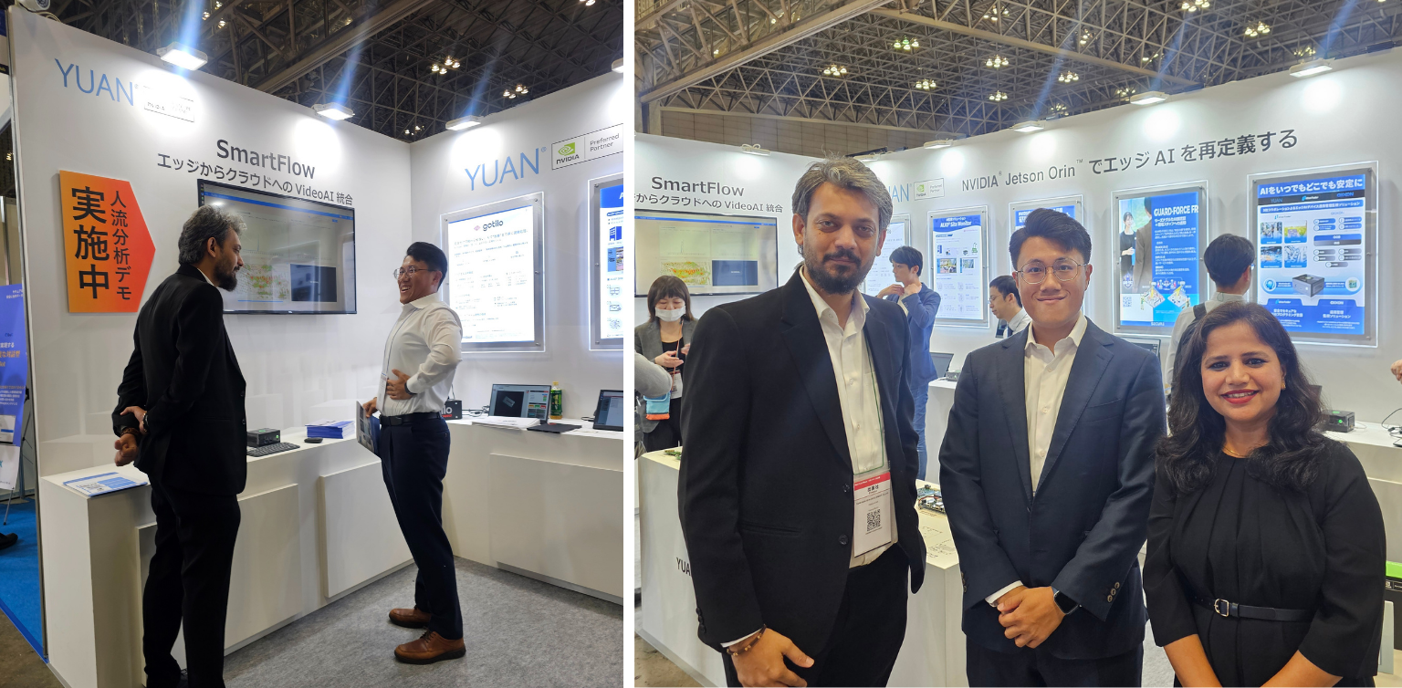
Inside the Gotilo-verse

Every few decades, an idea reshapes how industries perceive themselves.

Not through disruption, but through understanding.

The Gotilo-verse was born from such an idea, the belief that visibility can become the foundation of intelligence. It isn’t a platform or a product line; it’s an evolving world of AI Vision systems that learn, adapt, and translate visual reality into measurable logic.

For years, technology has promised automation. But automation alone is blind. It performs without context. The Gotilo-verse introduces a different kind of intelligence, one that watches first, then decides. It gives sight to environments that were once silent: a factory floor, a shipping dock, a parking structure, a warehouse aisle.

In this ecosystem, each solution becomes a living node of awareness. A camera at a manufacturing line understands quality in motion, noticing surface flaws invisible to the human eye. A vision system in a logistics yard identifies containers, tracks dwell time, and improves throughput without requiring new sensors. Retail outlets study shelf stock and foot traffic in real time. Farms analyze plant growth by light reflection and leaf pattern.

Every setting becomes a new dimension of the Gotilo-verse, distinct in purpose, connected by vision.

What makes this universe remarkable isn’t its scale, but its sensitivity. It’s the ability to think where the work happens, not in distant servers, but at the edge. Each frame processed becomes a decision made locally, instantly, and intelligently.

For emerging markets, this shift is transformational. They no longer need to choose between affordability and sophistication. Vision AI offers both, precision that scales without excessive infrastructure, insight that grows without complexity.

The Gotilo-verse, in essence, is not about building smarter machines. It’s about creating calmer ones, systems that observe carefully, decide wisely, and act only when needed.

Because the future of technology will not be defined by how fast it reacts, but by how deeply it understands.

And that understanding always begins with seeing clearly.

Until the Next Time…

This month, we spoke of vision in action, from Japan’s exhibition floors to the growing landscape of the Gotilo-verse, where AI is learning not just to detect, but to understand. We explored precision, patience, and the quiet intelligence that defines our future.

As November begins, we carry these ideas forward to Anaheim, ready to turn insight into impact once again.

The Technical Anatomy of a Parking Twin

Every city breathes in patterns.

Cars move, pause, and disperse in a rhythm that repeats itself through hours and seasons. Beneath this rhythm lies a kind of language, the pulse of motion that defines how urban life organizes itself. Yet, for all the technology that has reshaped cities, one of the simplest and most visible elements of infrastructure, the parking lot, often remains the least understood.

The Parking Twin was built to give this ordinary space a new intelligence. It translates movement into data, data into structure, and structure into clarity. It is not a concept that exists only in digital models or futuristic diagrams. It operates at ground level, reflecting the actual conditions of real environments.

At its core, the Parking Twin is a living digital reflection of a physical parking environment, created through the precision of Vision AI. It tracks the availability of every parking slot, observes the duration of each stay, and forms a continuously updated picture of occupancy patterns. The model provides visibility that is immediate, reliable, and easy to understand, visibility that begins exactly where it is needed.

Building Visibility from the Ground Up

A parking lot seems simple. Cars arrive, park, and leave. But when multiplied across hundreds or thousands of vehicles in a city, this simplicity becomes a complex system with measurable consequences, traffic congestion, wasted fuel, and reduced productivity.

Traditional approaches rely on sensors embedded in the ground or on periodic manual observation. These methods, while functional, often create fragmented insight. They record events but do not interpret them. The Parking Twin reimagines this process through the lens of Vision AI, where every movement is both observed and understood.

The system does not treat parking as an isolated task. It considers the entire flow, entry, stay, and exit, as a continuous process. Cameras placed strategically across a lot act as visual sensors, feeding video input into models trained to detect vehicles, recognize slot boundaries, and monitor time spent. Every slot becomes an intelligent node, aware of its status in real time.

What makes the Parking Twin unique is its grounding. Intelligence resides at the location itself. Processing happens near the source of data, reducing delay and ensuring the system reacts to the present, not to a delayed version of it. This is visibility built from the ground up, precise, local, and instantly verifiable.

The Core Framework of a Parking Twin

The design of the Parking Twin follows a clear logic. Like any digital twin, it mirrors the physical world in a virtual layer, but its focus remains on clarity over complexity. The system is composed of four interconnected layers, each performing a distinct function yet unified in purpose.

1. The Vision Layer – Capturing Reality

The foundation of the Parking Twin begins with the camera. Each camera becomes an intelligent eye, observing parking slots continuously and capturing the smallest variations in movement. Vision models trained under diverse lighting and weather conditions identify vehicles, classify them, and detect whether each slot is occupied or empty.

The model functions on pattern recognition rather than simple detection. It understands spatial relationships, where one slot ends and another begins, and tracks transitions. In practice, this allows it to distinguish between temporary pauses and actual parking events, creating a level of accuracy far beyond traditional sensors.

This layer does not depend on specialized hardware or pre-installed markers. Its adaptability allows it to integrate into existing parking infrastructure, transforming ordinary cameras into precise instruments of visibility.

2. The Processing Layer – Intelligence at the Source

Once visual data is captured, it is processed directly at the edge. This decision-to-process locally was guided by a simple engineering principle: clarity should not travel miles to be confirmed. Local computation minimizes latency, reduces bandwidth use, and strengthens privacy. The closer the data stays to its origin, the faster and more secure the result.

The processing layer performs inference, interpreting visual input in real time. It converts frames into structured data, classifies the occupancy state of each slot, and timestamps each event. This means that by the time information reaches the display or dashboard, it has already been analyzed and validated.

The advantage of this architecture lies in its efficiency. The model can continue operating seamlessly even when connectivity is inconsistent. The intelligence lives in the environment itself, ensuring that visibility remains constant.

3. The Analytical Layer – Measuring Movement

The analytical core of the Parking Twin interprets motion over time. Each parking slot becomes an ongoing data stream. The system records not only whether a slot is occupied but how long it remains in that state. These measurements are grouped into dwell time brackets, seconds, minutes, or hours, forming a complete picture of utilization.

By studying dwell time patterns, operators can identify zones with higher turnover, periods of peak demand, or underused areas within large facilities. The data reveals inefficiencies and supports planning decisions that were previously based on assumption.

The analytics layer serves both as a live monitoring tool and as a learning system. Over time, accumulated data builds predictive value, enabling facility managers to optimize layout, guide vehicles more efficiently, and reduce operational overhead.

4. The Visualization Layer – Clarity in Motion

The final layer of the Parking Twin is where insight becomes visible.
The dashboard translates technical complexity into simple visual language, color-coded maps, live occupancy indicators, and dwell time analytics. Each slot is marked by status:

  • Green: Available
  • Red: Occupied
  • Orange: Extended dwell or alert condition

The interface is designed for immediate comprehension. A single glance provides a complete operational picture. The clarity of visualization is not decoration; it is part of the engineering philosophy. A system achieves real value only when its information can be grasped instantly by the people who rely on it.

In addition to live tracking, the dashboard supports historical data exploration and anomaly detection. It becomes not only a monitoring tool but a decision instrument, one that connects observation to action.

The Design Philosophy – Engineering for Understanding

Technology often moves faster than understanding. The design of the Parking Twin was guided by a different pace, one that values refinement and simplicity over constant expansion. Every feature exists to make the invisible visible, not to overwhelm the user with data.

The guiding idea was clarity as a form of engineering discipline. The team behind the system defined success not by the number of features but by how quickly a person could read and interpret information. If a user could glance at the dashboard and know, without explanation, what was happening in a facility, the model had achieved its goal.

This philosophy mirrors the larger shift occurring in Vision AI, a move toward functional intelligence, where systems explain themselves through design rather than documentation. When data becomes understandable, it also becomes useful.

Demonstration in Motion – Real Validation

During the recent Japan IT Week 2025 exhibition, the Parking Twin was presented as a live working model. The event brought together engineers, integrators, and decision-makers from across industries, all seeking practical forms of AI integration.

Many were drawn to the simplicity of its logic, a structure that required no specialized hardware, no complex calibration, and minimal maintenance. The system’s design invited interaction; its clarity became the most convincing argument for its value.

For the WebOccult and Gotilo teams, the exhibition served as validation that Vision AI has entered its operational phase, a point where technology transitions from research to reliability. The model’s performance demonstrated that when design and intelligence align, the result feels natural, not mechanical.

Expanding the Framework – Beyond Parking

Although the current model focuses on parking management, the framework extends to a range of industrial and civic environments. The same architecture that tracks vehicles can monitor containers in a logistics yard, pallets in a warehouse, or assets in an industrial facility.

The digital twin principle, mirroring the real world in a living, measurable form, can be adapted to any domain where visibility leads to efficiency. The Parking Twin serves as a starting point, a demonstration of what happens when Vision AI is applied not to prediction, but to presence.

When visibility becomes immediate, human supervision changes its nature. Managers spend less time searching for information and more time acting on it. Systems designed with this philosophy free people from routine observation, allowing them to focus on interpretation and improvement.

The Broader View – Visibility as a Foundation

The Parking Twin reflects a growing movement in infrastructure design, the recognition that clarity itself is infrastructure. Cities are not only collections of roads and buildings but also of information pathways. Each new layer of visibility adds structure to the systems beneath it.

As data becomes a shared resource, the question shifts from “how much can we collect” to “how well can we understand what we see.” Vision AI provides the bridge between these questions. It transforms images into relationships, movement into metrics, and space into an organized sequence of decisions.

The Parking Twin is not a complete destination. It is an evolving proof of how intelligence can operate quietly, continuously, and independently. Its worth lies not in spectacle but in subtlety, in showing that the path to smarter infrastructure begins with understanding what already exists.

Looking Ahead – The Future of Measurable Intelligence

As technology advances, the goal is not to automate more but to understand more precisely. The next stage for systems like the Parking Twin lies in learning through accumulation, using historical data to refine future awareness.

Dwell time patterns can inform predictive guidance, adjusting layouts based on usage density. Integration with traffic and logistics systems can expand its role beyond parking lots into transport networks. With each application, the same foundation remains: visibility, measurement, and reliability.

The evolution of such systems will depend less on invention and more on refinement, on making technology quiet, dependable, and harmoniously present in the environment.

Closing Reflection – Seeing as Structure

Visibility is not decoration. It is structure. In engineering, as in design, the act of seeing forms the basis of control. The Parking Twin represents that principle made tangible, a space observed, understood, and continuously synchronized with its digital counterpart.

Each frame captured by the camera contributes to an ecosystem of understanding. Every slot detected becomes a small node of order in the larger system of movement. Over time, these small pieces form an invisible architecture that supports the visible one.

This is the essence of measurable intelligence, not to replace human perception but to strengthen it. When technology begins to see with purpose, human decisions gain depth.

The Parking Twin stands as proof of this quiet shift. It shows that clarity can be engineered, that systems can think in rhythm with the world they observe, and that progress begins the moment we choose to see with precision.

Every innovation begins with a conversation.
The Parking Twin was designed not as a finished product, but as an invitation to reimagine how visibility supports performance.

At WebOccult | Gotilo, we continue to refine solutions that connect Vision AI with the real conditions of modern industry, in manufacturing, logistics, infrastructure, and urban operations. Each project is built with the same philosophy: to measure meaningfully and to deliver clarity that lasts.

If your organization is exploring ways to make operations more transparent, predictable, and measurable, we invite you to start a dialogue.

Connect with our team at www.weboccult.com

Semiconductor Fab in 2025 – Key Trends in Vision AI & Inspection Technologies

Walk into a semiconductor fabrication plant in 2025 and you’ll see something that looks more like a science fiction set than a factory. Robots glide across spotless cleanrooms, wafers are carried through vacuum-sealed chambers, and machines whisper in precision rhythms. Each wafer that enters the fab is a canvas on which billions of transistors will be etched, stacked, and polished.

But behind this incredible story of machines lies a truth: fabs are under immense pressure. Every new generation of chips is harder to make. Transistors are now so small that thousands could fit across the width of a human hair. Processes that were once manageable by traditional inspection are now too complex, too fast, and too unforgiving. A single microscopic flaw, smaller than a virus, can ripple through thousands of wafers and cost millions of dollars in yield losses.

This is why 2025 is different. This is the year when inspection in fabs shifts decisively from being a checkpoint to being the nervous system of manufacturing. Computer vision, paired with deep learning and automation, is no longer optional, it’s essential. This rise of Vision AI in wafer fabs is one of the defining Semiconductor fab trends 2025, transforming how defects are found, predicted, and prevented.

In the sections ahead, we’ll explore why inspection matters more than ever, how AI is reshaping it, the trends driving the change, and what the fab of the future looks like.

Why Vision AI Matters Now

Semiconductor fabs have always been about precision. But the level of precision required in 2025 is unlike anything seen before.

Each chip today may contain over 100 billion transistors. The photomasks used to print patterns are more complex than city maps. Layers stack one on top of another, sometimes more than 80 deep, each requiring flawless alignment. And as architectures like 3D ICs and chiplets become more common, even vertical stacking must be perfect.

The problem is that traditional inspection tools, optical microscopes, rule-based automation, or manual review, cannot keep up. They either miss tiny defects or overwhelm engineers with false alarms. Worse, they are reactive: they tell you a defect has occurred, but not how to stop it from happening again.

By contrast, AI inspection semiconductor systems work differently. They don’t just scan wafers; they learn from them. They analyze massive datasets of wafer images, detect patterns humans can’t see, and predict issues before they cascade. They can operate in real time, ensuring that problems are corrected on the fly rather than after the fact.

In short: AI doesn’t just give fabs new tools. It gives them new eyes, and in many cases, a new brain.

Key Vision AI & Inspection Trends in 2025

Now let’s explore the defining trends of 2025, how inspection technologies powered by AI are rewriting the rules of semiconductor manufacturing.

1. Predictive Defect Detection

In older fabs, inspection was like looking in the rearview mirror: you saw defects after they happened. But by then, dozens of wafers were already damaged.

In 2025, inspection has become predictive. By analyzing patterns across thousands of wafers, AI systems can forecast problems before they appear. For example, subtle changes in slurry flow during CMP polishing can signal erosion risks. Tiny irregularities in plasma glow can warn of etching drift. AI systems catch these warning signs and alert operators, or even adjust processes automatically, before defects spread.

This shift to predictive defect detection is saving fabs millions each year. Instead of reacting to yield losses, fabs now prevent them. It’s like moving from a doctor who treats illnesses to one who predicts them and keeps you healthy.

2. Edge AI in Semiconductor Inspection

Inspection creates enormous amounts of image data. A single wafer scan can generate terabytes of information. Sending all of this to cloud servers for processing is slow and risky.

That’s why in 2025, more fabs are deploying Edge AI in semiconductor lines. Processing happens directly at the tool, right where wafers are polished, etched, or patterned. This reduces latency, ensures immediate feedback, and keeps sensitive design data secure.

For time-critical processes like etching, CMP, or resist coating, edge AI is a game-changer. Decisions that once took minutes now happen in seconds.

3. Fab Automation Trends

Fabs are also moving toward greater automation. But automation in 2025 isn’t just about robots moving wafers, it’s about inspection systems that take corrective action on their own.

These fab automation trends include closed-loop systems. Imagine CMP polishing: if AI vision detects early signs of dishing, it can automatically adjust pad pressure or slurry flow. In lithography, if overlay drift is detected, exposure parameters can be corrected instantly.

This automation turns fabs into self-healing systems, reducing reliance on manual intervention and cutting downtime.

4. Multi-Stage Vision AI Integration

Until recently, fabs treated inspection as siloed steps. There was one system for photomasks, another for CMP, another for packaging. Each step generated data, but that data rarely connected.

Now, AI is integrating inspection across the entire fab. Results from photomask inspection inform wafer-level monitoring. CMP data feeds into packaging checks. By connecting dots across the process, fabs can find root causes faster and optimize workflows holistically.

This multi-stage integration is a stepping stone to future semiconductor inspection, where data from across fabs is unified into one intelligent system.

5. Smarter Defect Classification

Another big trend in 2025 is smarter classification. Instead of simply labeling a wafer as good or bad, AI systems categorize defects precisely: scratches, pits, voids, erosion, bubbles.

Knowing the type of defect helps fabs respond quickly. A scratch might mean maintenance on pads. A void could indicate process gas instability. Erosion might require slurry adjustments. By giving context, AI turns inspection from a red flag into actionable insight.

This is one of the quiet revolutions of 2025, inspection isn’t just about detection anymore. It’s about diagnosis.

6. Sustainability and Yield Optimization

Sustainability is also shaping inspection trends. Fabs consume huge amounts of water, chemicals, and energy. Every defective wafer means wasted resources.

By improving yields and reducing scrap, Vision AI helps fabs lower both costs and environmental impact. Some fabs report that AI monitoring of CMP and resist coating cut chemical usage by 10-15%. Others note that predictive maintenance reduced downtime, saving both energy and materials.

In an industry under pressure to balance growth with responsibility, this is a major win.

Challenges in 2025

Even with these advances, challenges remain.

  • Data volume: Each wafer generates terabytes of inspection images. Managing and analyzing this at scale requires hybrid architectures combining edge and cloud.
  • Integration: Connecting AI inspection with MES, yield management, and process control systems is complex but essential.
  • IP security: Fabs must protect design data when training AI models.
  • Continuous retraining: AI models must evolve as new nodes, materials, and defect types emerge.

Despite these hurdles, investment is accelerating. Fabs know that without Vision AI, they risk falling behind.

The Future of Semiconductor Inspection

Looking ahead, inspection will become the fabric of fabs, not just a feature.

Future semiconductor inspection will be:

  • Proactive: predicting and preventing defects, not just finding them.
  • Integrated: linking data across tools, fabs, and even global supply chains.
  • Autonomous: working hand in hand with robots and process tools to create truly self-healing fabs.
  • Sustainable: cutting waste and optimizing resources.

The vision is a fab where defect-driven yield loss is near zero, where wafers move through processes guided by intelligent systems that see everything and act instantly.

At WebOccult, we see inspection as more than quality control, it’s the foundation of semiconductor automation.

Our solutions combine deep learning, edge processing, and seamless integration to give fabs real-time insights at every step. We help manufacturers implement AI inspection semiconductor systems that predict problems, enable closed-loop control, and scale across nodes.

Whether it’s photomask inspection, CMP monitoring, overlay accuracy, or packaging validation, our vision based inspection platforms are designed for precision, adaptability, and reliability.

As fabs evolve into smart fabs, WebOccult is here to help them achieve higher yields, lower costs, and greater confidence in every wafer produced.

Conclusion

The semiconductor industry in 2025 is both more exciting and more demanding than ever. Chips are powering AI, 5G, autonomous vehicles, and more. But manufacturing them has never been harder. Traditional inspection cannot keep up.

Vision AI in wafer fabs has become the guardian of this new era. It predicts defects, enables real-time corrections, and connects data across processes. It reduces waste, improves yield, and makes fabs smarter and more sustainable.

In the landscape of Semiconductor fab trends 2025, inspection is not a footnote, it’s the headline. It is the key to unlocking smaller nodes, advanced architectures, and reliable supply chains.

At WebOccult, we believe that in the race for precision, inspection is not just about what you see, it’s about what you can predict, prevent, and perfect. That is the promise of Vision AI, and that is the future of semiconductor manufacturing.

How Computer Vision Is Transforming Semiconductor Fabrication Plants

Semiconductor fabrication plants, commonly called fabs, are some of the most complex and expensive factories ever built. Inside cleanrooms that are thousands of times cleaner than a hospital operating room, wafers of silicon are transformed into chips that power the world’s smartphones, cars, medical devices, and satellites.

Every wafer goes through hundreds of steps, lithography, deposition, etching, polishing, packaging, and at each step, there is zero tolerance for mistakes. A single defect invisible to the human eye can multiply across millions of transistors and render an entire batch of chips useless. With advanced fabs costing billions of dollars to build and wafers worth thousands each, failure is not an option.

For decades, engineers relied on human inspection, microscopes, and rule-based automation to monitor wafers. But as technology nodes have shrunk from 90nm to 7nm, 5nm, and now 3nm, and with 2nm on the horizon, the old methods are no longer enough. Patterns are too complex, tolerances are too small, and the stakes are too high.

This is where computer vision in semiconductor manufacturing is changing the game. By combining ultra-high-resolution cameras with deep learning and automation, computer vision has become the new eyes of the fab. It enables real-time monitoring, faster decision-making, and higher accuracy than humans or legacy tools can achieve. From AI wafer inspection and overlay accuracy to CMP monitoring and packaging validation, vision based inspection is now at the heart of semiconductor automation.

Together, these technologies are giving rise to a new generation of smart fabs, factories that are not only faster and cleaner but also intelligent and adaptive.

Why Precision Matters in Semiconductor Manufacturing

To understand why fabs are embracing computer vision, we need to appreciate just how unforgiving semiconductor manufacturing is.

Each chip contains billions of transistors packed into a space smaller than a fingernail. A single defect, such as a scratch, a particle of dust, or a misaligned pattern, can cause a chip to fail. And because wafers are processed in lots, one defect can spread across hundreds of chips, costing millions of dollars in losses.

Photomasks, for example, act as the stencils for circuit patterns. If a photomask has a defect, that flaw is repeated across every wafer it prints. Similarly, if CMP polishing leaves a wafer slightly uneven, every subsequent layer is affected. If plasma etching goes too deep or too shallow, entire circuits may be ruined.

In short, precision is everything. And the smaller the node, the less room there is for error. This is why fabs are now investing heavily in semiconductor fabrication AI, to ensure that even the tiniest issues are caught and corrected before they cause large-scale yield loss.

Where Computer Vision Makes an Impact

Computer vision is no longer limited to a single inspection step. It is now present across almost every stage of semiconductor manufacturing. Let’s explore the key areas where it makes the biggest difference.

1. Photomask Defect Inspection

Photomasks are the master blueprints for chips. Traditional inspections often missed defects at the sub-30nm scale. Now, AI-driven vision systems can scan masks at extreme resolution, catching defects like pinholes, scratches, or contamination before they spread to wafers. This improves yield and prevents costly rework.

2. Alignment and Overlay Accuracy

As layers are stacked on top of one another, even a nanometer misalignment can cause electrical failures. Vision systems constantly monitor overlay accuracy, ensuring patterns line up perfectly. This is critical as fabs move to EUV (Extreme Ultraviolet) lithography, where tolerances are razor-thin.

3. CMP (Chemical Mechanical Planarization) Monitoring

CMP polishes wafers flat between layers, but it can also introduce dishing, erosion, and scratches. Vision systems analyze wafer surfaces post-CMP, detecting non-uniformity in real-time. This prevents defects from compounding across dozens of layers.

4. AOI (Automated Optical Inspection) for PCBs and Modules

Once wafers are processed into modules or PCBs, vision systems check for open circuits, soldering faults, and missing components. AI wafer inspection at this stage ensures that packaging errors don’t undo the precision of earlier steps.

5. Plasma Etching Endpoint Detection

Etching defines the fine features of a chip, but stopping too early or too late can ruin circuits. Computer vision systems analyze plasma glow patterns in real time, ensuring etching ends exactly when it should.

6. Resist Coating and Film Uniformity

Photoresist coating must be perfectly even. Vision-based inspection detects film thickness variations or surface contamination during coating, ensuring lithography accuracy.

7. Packaging and Assembly Validation

In advanced packaging like Package-on-Package (PoP), vision systems ensure vertical alignment and connection integrity before reflow. This prevents latent defects that may only appear later in use.

8. Defect Classification and Sorting

Instead of just flagging problems, modern vision systems categorize them, scratches, voids, pits, bubbles, so fabs can find root causes faster. This accelerates problem-solving and improves long-term yields.

Together, these use cases show how vision systems act as the silent guardians of fabs, watching every process, every wafer, every layer.

The Benefits of Computer Vision in Fabs

The impact of computer vision is more than just catching defects. It changes the economics and efficiency of semiconductor manufacturing.

  • Nanometer Accuracy: Detects defects invisible to traditional tools.
  • Real-Time Monitoring: Prevents cascading failures before they spread.
  • Higher Yield: More wafers pass final tests, boosting profitability.
  • Consistency: Removes human subjectivity and fatigue.
  • Cost Savings: Avoids multi-million-dollar losses per defect lot.
  • Scalability: Adapts to 28nm, 7nm, 3nm, and future 2nm nodes without reprogramming.

One report suggests that fabs using vision based inspection and semiconductor fabrication AI have seen yield improvements of 20–30%, translating to hundreds of millions of dollars in savings each year.

Real-World Examples & Industry Trends

The world’s leading fabs are already adopting these technologies.

  • TSMC uses AI inspection to manage the complexities of EUV lithography.
  • Samsung has integrated AI monitoring in its 3nm Gate-All-Around processes.
  • Intel has deployed deep learning for faster defect classification, cutting manual review times significantly.

In one case study, a fab that piloted AI-based CMP monitoring reported a 25% reduction in defect escapes and a 40% faster inspection cycle time. Another fab saw false positives drop by over 30%, freeing engineers to focus on real problems.

The analogy is clear: traditional inspection is like using a magnifying glass; AI-driven computer vision is like running an MRI scan. It sees deeper, faster, and with more context.

Challenges and Considerations

Adopting computer vision across fabs isn’t without hurdles.

  • Data Volume: High-resolution imaging produces massive data streams. Processing them requires edge computing near tools, often combined with cloud analytics.
  • Integration: AI outputs must connect smoothly with lithography machines, MES systems, and yield management platforms.
  • Security: Wafer designs and defect libraries are highly valuable IP. Systems must ensure confidentiality.
  • Continuous Learning: As fabs introduce new materials and nodes, AI models need retraining.

Despite these challenges, the momentum is clear. The benefits far outweigh the barriers, and fabs are finding ways to integrate vision systems at scale.

The Future of Computer Vision in Semiconductor Fabs

The future lies in smart fabs, factories where vision systems not only detect defects but also correct processes automatically.

  • Closed-Loop Manufacturing: Vision systems detect an issue and adjust polishing, etching, or coating in real time.
  • Predictive Maintenance: AI predicts when tools need servicing before defects occur.
  • 3D ICs and Chiplets: As designs move toward stacked chips, vision will be critical for ensuring perfect alignment.
  • Zero-Defect Ambition: With continuous monitoring, fabs are moving toward defect-free manufacturing.

In short, computer vision is turning fabs from reactive factories into intelligent, semiconductor automation ecosystems.

WebOccult’s Role in Fab Transformation

At WebOccult, we understand that semiconductor fabs are under pressure like never before, shrinking nodes, tighter tolerances, higher costs, and massive demand. Our AI Vision solutions are built to help fabs navigate this challenge.

  • We provide AI wafer inspection tools that catch the smallest defects.
  • Our systems are designed for real-time, vision based inspection, ensuring immediate feedback.
  • We build platforms that integrate seamlessly into fab workflows, supporting semiconductor automation without disruption.

By combining expertise in computer vision in semiconductor manufacturing with deep industry knowledge, WebOccult delivers not just technology but a path to higher yield, lower costs, and smarter fabs.

Conclusion

The semiconductor industry has always balanced ambition and precision. As ambition drives us to smaller, faster, more powerful chips, precision becomes more unforgiving. At this level, a dust particle can be a villain, a scratch can be a disaster, and a single defect can cost millions.

Computer vision has become the watchtower of fabs. It ensures that defects are caught early, surfaces remain flat, patterns align perfectly, and packaging is precise. It turns fabs into smart fabs, intelligent, adaptive, and resilient.

In the race to advance Moore’s Law, computer vision in semiconductor manufacturing is not just a tool. It is the shield protecting yields, the compass guiding defect detection in chips, and the foundation of semiconductor automation.

At WebOccult, we are proud to help fabs take this leap. With AI-driven vision, we help manufacturers move closer to defect-free production, ensuring that every chip, every wafer, and every layer meets the standards of the future.

WebOccult Insider | Sep 25

Introducing, Gotilo!

An AI Vision Platform of WebOccult

Some milestones arrive with fanfare. Others arrive quietly, shaping themselves piece by piece, until one day you realize, something bigger is taking form.

That’s where we are today. WebOccult and Gotilo are in the middle of building one unified product arm.

It isn’t a press release moment, it’s a work-in-progress. But it’s also a turning point.

For years, WebOccult has been at the frontier of AI Vision and intelligent automation, while our prodcut arm Gotilo has been designing products and digital-first experiences.

Now, these journeys are bending towards each other. Not merging overnight, but aligning steadily , with one goal: to create products that don’t just solve problems, but set new standards.

Together, we’re shaping a product DNA that values:

  • Accurate, Solve measurable problems.
  • Adaptive, From edge to enterprise.
  • Assured, Privacy, governance, reliability.

This story is still being written. The lines aren’t finished, but the direction is clear:

One arm. One vision. Infinite possibilities.


Clarity at Every Scale

When I think about the journey of our work, I often return to one idea: clarity. In ports, that meant giving operators the ability to see where a container was, how long it had stayed, and what condition it was in. That clarity turned movement into order.

Now, our attention has moved to semiconductors, too. This industry carries a different kind of weight. A port can lose hours and recover(still not recommended:)). A factory making microchips cannot afford a single unnoticed error. One particle of dust, one fracture thinner than a hair, and weeks of work collapse into waste.

Precision is not optional. It is survival.

In this space, I believe computer vision can play a decisive role. Imagine inspection systems that do not pause the line, yet catch a surface crack the instant it forms. Systems that can detect the faintest contamination before it

spreads, or verify the alignment of patterns across layers without human delay. These are not dreams. They are the kind of tools our team is building with care and discipline.

At the same time, there is another story unfolding. WebOccult and Gotilo are drawing closer, preparing to stand as one product arm.

This process is not a single announcement. It is a gradual alignment, step by step, where our focus on vision and Gotilo’s craft in product design begin to share the same rhythm.

The work is still in progress, and I will speak more of it in the months ahead.

For now, I can say this much: it is about giving our products one voice, one structure, and one standard of intent.

That is the path forward.

The Next Layer of Vision: Context in Semiconductor Inspection

In ports, cameras were asked to track movement. They followed trucks as they entered, containers as they shifted, and gates as they opened or closed. The question was direct: did something move, and where did it go? When vision turns toward semiconductors, that question no longer suffices. Here, the challenge is not motion but detail.

A fracture smaller than a hair or a line drawn out of alignment may not be visible to the human eye, yet it can render an entire wafer useless.

The work of inspection, then, is not limited to noticing whether a defect exists. It requires knowing the conditions in which the defect appears. A mark on the surface may be harmless if it belongs to a permitted stage, but alarming if it emerges in the wrong layer, at the wrong temperature, or during the wrong process. In such an environment, detection without interpretation is incomplete.

Context decides whether the observation is trivial or decisive.

Such progress marks a shift from reactive inspection to predictive insight. It is no longer about responding to an error once it halts production. It is about anticipating the fault before it spreads and halting it at its source. For semiconductors, this difference is critical. A port can lose an hour and recover.

A fabrication line that loses precision risks months of loss. In this field, certainty is not an advantage. It is survival.

Offbeat Essence – The Value of Pausing

Patience is also intelligence, for it teaches us that not every signal deserves a response.

AI systems are often praised for speed. They do not blink, they do not tire, and they can run through millions of frames without hesitation. But sometimes, intelligence is found not in rushing, but in pausing.

In our work with vision systems, we have begun to see the value of deliberate stillness. A frame is not just an image; it is a moment in time. If the system moves too quickly, it may treat every flicker of light as a fault, every passing shadow as a threat. By learning when to pause, an AI can measure more carefully, judge more calmly, and ignore noise that distracts from truth.

This ability to wait, even for a fraction of a second, brings balance. It reflects something deeply human as well: knowing when to act, and when to let a moment pass. For AI vision, the lesson is clear. The goal is not endless attention, but meaningful attention.

Because seeing everything is not the same as understanding what matters.

Three Days in Ranakpur: A Journey Remembered

Our journey began with a halt at Nathdwara. The darshan there gave us a calm start, a pause before the road stretched again toward the Aravalli hills. The bus ride that followed carried its own spirit. Songs played, people talked, and laughter moved from one row to another until the long road seemed shorter. By the time we reached, the shift was already felt.

The evening brought jeep rides through the forest, where dust and wind filled the air, and later, the pool offered a quieter break. It was a day that moved between energy and ease.

The second morning began differently. We set out for the Ranakpur Dam, walking through paths that opened into still water and quiet hills. That calm stayed with us, but soon the day turned lively. Games filled the afternoon, Mystery Box, Passing Powder, and a Scavenger Hunt that sent everyone running in groups. These small challenges were not about winning or losing but about seeing each other outside the usual setting of work.

Jokes grew, laughter spilled, and the team felt lighter. As evening fell, the DJ night began. Music and dance carried the group into another rhythm, one where effort and release met on the same floor.

On the third day, the trip began to fold back into itself. Bags were packed, seats taken, and the road to Ahmedabad stretched once again before us. Yet the journey felt different this time. The bus was quieter, the conversations softer, as if everyone carried something unspoken. Journeys back often feel shorter because the memories already begin to fill the space.

Looking back, it is clear that such trips are not measured by distance. They stay with us in stories, in small shared moments, in a sense of belonging that grows stronger when people spend time side by side. Ranakpur gave us that gift, and it will remain part of our story long after the road dust has settled.

On the Path Ahead

Japan | Next Tech Week
(8–10 October, 2025)
Co-exhibiting with YUAN

Japan | IT Week
(22–24 October, 2025)
Co-exhibiting with Deeper-i

USA | Embedded World
(4–6 November, 2025)
Co-exhibiting with YUAN

USA | Embedded World
(4–6 November, 2025)
Co-exhibiting with Beacon Embedded + MemryX

Until the Next Time…

his month, we spoke less of finished milestones and more of journeys in motion. The idea of one product arm between WebOccult and Gotilo is taking shape step by step, not yet announced in full but already guiding how we think about what we build.

As we close this issue, we look ahead with the same intent: to keep refining our products, to learn when to act and when to pause, and to build together with care.

See you in the next edition, with sharper tools, steadier vision, and a deeper sense of purpose.

AI Vision in Chemical Mechanical Planarization (CMP) Quality Monitoring

Every chip in your phone, your laptop, or even in a satellite, begins as a plain slice of silicon. But before that slice can become the heart of advanced electronics, it has to go through a series of complex processes. One of the least understood, yet most critical of these, is called Chemical Mechanical Planarization, or simply CMP.

CMP is not a flashy process. It doesnt involve lasers carving patterns or robots assembling wafers. Instead, it does something deceptively simple: it polishes wafers to make them perfectly flat. Imagine trying to build a skyscraper on uneven ground, no matter how well you design the upper floors, the entire structure will be unstable. CMP ensures that every new layer of a chip is built on a perfectly flat foundation.

But heres the catch: CMP itself can introduce defects. A little too much pressure, an uneven polish, or slight wear in the pad can cause problems like dishing, erosion, or scratches. These are tiny imperfections, but in a chip where billions of transistors are packed together, even the smallest flaw can disrupt performance.

For decades, fabs relied on traditional ways to monitor CMP, such as checking sample wafers or measuring thickness with offline tools. But those methods cant keep up with todays demands. Chips have dozens of layers, each requiring precise planarization. Missing a defect at one layer means problems multiply across the rest. This is why fabs are turning to AI Vision systems, technology that can see, analyze, and react in real-time to keep CMP under control.

AI Vision in CMP isnt just an upgrade. Its a transformation. It takes what was once a slow, error-prone process and turns it into a smart, adaptive, and almost self-correcting step in semiconductor manufacturing.

CMP robotic wafer polishing equipment semiconductor fabrication

Why CMP is Critical in Semiconductor Manufacturing

To understand why AI matters, we first need to understand why CMP is so important.

Chips are not made in one go. They are built layer by layer, sometimes stacking more than 50 or even 80 layers of metal and dielectric materials. Each new layer must sit perfectly on the previous one. If the surface isnt flat, two problems occur:

  • Patterns dont line up properly (overlay errors).
  • Electrical connections fail because wires are too thin or too thick in certain areas.

CMP ensures that after each deposition or etching step, the wafer surface is polished flat before moving to the next. Without this step, chips would quickly fail.

But CMP itself is delicate. Problems include:

  • Dishing: When soft materials like copper are polished more than surrounding harder areas, leaving shallow pits.
  • Erosion: When large areas lose too much material, making surfaces uneven.
  • Scratches: Introduced during polishing, which can cause open circuits.
  • Non-uniform thickness: When one part of the wafer is polished differently from another.

These issues might sound minor, but in semiconductors, they are catastrophic. A single CMP defect can cause entire wafers to be scrapped. Studies show that CMP-related issues can account for nearly 30-40% of yield loss in advanced fabs.

With each wafer worth thousands of dollars, and each lot worth millions, fabs cannot afford such losses.

The Limits of Traditional CMP Monitoring

For years, fabs have used a mix of manual inspections, sampling, and offline measurements to monitor CMP quality. While these methods worked reasonably well in older technology nodes, they are showing cracks as the industry pushes forward.

  • Sampling is incomplete: Only a few wafers are checked out of hundreds. Defects on unchecked wafers may go unnoticed until much later.
  • Manual inspection is slow: Engineers cannot keep up with the sheer number of wafers and layers.
  • Time-based control is unreliable: CMP is often run for a fixed duration, assuming uniformity. But real-world conditions vary, pad wear, slurry condition, and tool vibration all affect outcomes.
  • Feedback is delayed: By the time a defect is found, dozens of wafers may already be damaged.

This reactive approach is costly. Instead of preventing defects, fabs often discover them only after theyve caused irreversible losses.

How AI Vision Transforms CMP Quality Monitoring

AI Vision brings a new way of thinking. Instead of waiting to check wafers after polishing, it continuously monitors CMP surfaces in real-time.

Heres how it works:

  • High-resolution imaging systems capture wafer surfaces immediately after polishing. These systems are sensitive enough to detect tiny changes in reflectivity, texture, and thickness.
  • AI models analyze the images, comparing them to vast libraries of defect patterns. They can distinguish between a harmless variation and a true defect like dishing or erosion.
  • Real-time feedback loops connect the AI system to the CMP equipment. If the AI detects an uneven polish, the process can be adjusted instantly, slurry flow, pad pressure, or polishing time can be fine-tuned on the fly.
  • 100% inspection coverage becomes possible. Instead of sampling a few wafers, AI vision can analyze every wafer, every time.

The result is a shift from reactive to proactive. Instead of discovering CMP problems after yield loss, fabs can prevent them before they happen.

Benefits of AI vision in CMP

The Benefits of AI-Powered CMP Monitoring

The shift to AI Vision unlocks multiple advantages:

  • Real-time detection: No more waiting for offline results. Defects are caught immediately.
  • Higher yield: By preventing early CMP issues, subsequent layers are protected, ensuring stronger overall device reliability.
  • Reduced waste: Wafers no longer need to be scrapped after costly defects are discovered too late.
  • Consistency: Every wafer, not just samples, meets the same high-quality standard.
  • Cost efficiency: Less waste, fewer reworks, and higher throughput directly boost fab profitability.

Think of it this way: traditional monitoring is like inspecting a finished cake to see if its baked evenly. AI vision is like checking the oven conditions in real-time to ensure every cake comes out perfect.

Real-World Impact

The semiconductor industry has already seen the difference AI makes in CMP.

One fab introduced AI-based vision systems into its CMP line and reported a 25% reduction in defect escapes. Another noted that real-time monitoring helped them reduce polishing time per wafer, saving both cost and energy.

Fabs also discovered that AI could detect early warning signs of pad wear and slurry issues, things that traditional methods missed. This predictive capability means fabs can perform maintenance before defects occur, rather than after.

A senior engineer compared the shift to moving from looking in the rearview mirror to having a live GPS system. Instead of reacting to problems, fabs are guided to prevent them.

Challenges to Overcome

Of course, adopting AI Vision in CMP isnt without hurdles.

High-resolution imaging under polishing conditions is technically demanding. The equipment must handle slurry, vibrations, and harsh fab environments. The data generated is enormous, analyzing thousands of wafer images in real-time requires robust computing infrastructure.

Data security is also important. CMP recipes and defect libraries represent valuable intellectual property. Fabs must ensure AI models are trained and run in secure environments.

And finally, AI needs constant retraining. As new chip designs, new materials, and new processes emerge, AI must adapt. Building these continuous learning pipelines is both a challenge and an opportunity.

The Future of CMP Monitoring

Looking ahead, AI Vision is set to make CMP not just smarter, but nearly autonomous.

Future fabs will run closed-loop CMP systems, where AI doesnt just detect defects but automatically corrects processes in real-time. Polishing pads will adjust pressure dynamically, slurry flow will change based on surface conditions, and wafer flatness will be ensured without human intervention.

As 3D ICs and advanced packaging gain ground, the role of CMP will only grow. With multiple stacking layers and complex interconnects, the demand for flat, defect-free surfaces is higher than ever. AI will be the backbone ensuring this reliability.

The vision is clear: fabs where defects are not only caught but prevented, factories where yield loss from CMP becomes nearly zero.

AI vision system detecting wafer pattern misalignment

WebOccults Role in AI-Powered CMP Monitoring

At WebOccult, we understand that CMP is the foundation of every chip. Our AI Vision platforms are designed to monitor wafer surfaces in real-time, catch the smallest imperfections, and integrate seamlessly into fab workflows.

Our systems dont just detect problems, they help prevent them. With adaptive learning models, we ensure CMP monitoring evolves with each new process node. With robust integration, we ensure fabs dont face disruption but instead gain efficiency.

For fabs under pressure to deliver defect-free wafers at advanced nodes, WebOccult provides more than technology. We provide a partner committed to reducing waste, protecting yields, and enabling the semiconductor future.

Conclusion

Semiconductors may look like miracles of engineering, but they are built on something very basic: flatness. Without flat wafers, the most advanced chip designs would collapse. CMP, though invisible to most people, is the silent backbone of every chip ever made.

Yet CMPery nature makes it vulnerable to defects. Left unchecked, these defects multiply into huge losses. Traditional methods are no longer enough. AI Vision steps in as the watchful guardian, seeing in real-time, learning with each wafer, and ensuring every surface is as perfect as it needs to be.

In the journey to smaller and faster chips, CMP will remain the foundation. And AI Vision will ensure that this foundation stays strong.

At WebOccult, we are proud to help fabs flatten the path to the future, making CMP smarter, cleaner, and more reliable, one wafer at a time.

NVIDIA Jetson Thor

Powering the Next Era of Vision AI

Artificial Intelligence has moved from labs and data centers into the real world.

Today, cameras on highways are expected to analyze traffic, robots on factory floors make micro-second safety decisions, and drones survey farms with intelligence far beyond simple recording.

The challenge?

Edge devices have always been limited. They either lacked the raw horsepower to run advanced AI models, or they depended too much on cloud servers, which brought latency, bandwidth costs, and privacy concerns.

NVIDIAs new Jetson AGX Thor is designed to change that equation. With supercomputer-like performance in a compact module, Jetson Thor unlocks the ability to run heavy Vision AI workloads directly at the edge, where milliseconds matter most.

What exactly is Jetson Thor?

Jetson Thor is NVIDIAs most advanced embedded AI system yet, built on the Blackwell GPU architecture. It has been described as a supercomputer for robots and edge devices and not without reason.

At its core, Jetson Thor offers:

  • 2,070 TeraFLOPs of AI compute (FP4 precision), a 7— jump from Jetson Orin.
  • A 14-core Arm Neoverse CPU cluster for enterprise-grade computing.
  • 128 GB of LPDDR5X memory with blazing 273 GB/s bandwidth.
  • Support for 20 camera sensors with simultaneous high-resolution feeds.
  • Multi-Instance GPU (MIG) for workload partitioning and isolation.

To put it simply, Jetson Thor brings data center power into a module small enough to fit into a drone, a robot, or an on-site server box.

Jetson Thor vs Jetson Orin – Why This is a Leap

The Jetson Orin series has powered many of todays smart cameras, robots, and edge AI systems. But compared to Orin, Thor is a giant leap forward.

  • 7.5— more AI compute: From ~275 TOPS on Orin to over 2,000 TFLOPs on Thor.
  • 3— faster CPU performance: Thanks to the new Arm Neoverse cores.
  • 2— memory capacity: 128 GB vs. 64 GB.
  • 3.5— better performance per watt: Higher efficiency means more tasks with less energy.

This isnt just an upgrade, its a transformation. Where Orin could handle a handful of AI workloads at once, Thor can run multiple heavy models simultaneously, from video analytics to generative AI, without breaking a sweat.

Why Jetson Thor is Perfect for Vision AI

Computer vision is one of the most demanding AI workloads. Every frame of a video contains millions of pixels, and with multiple cameras streaming simultaneously, the processing requirements skyrocket. Add to that the need for real-time responses, and you see why the edge has struggled.

Heres where Jetson Thor makes the difference:

1. Real-Time Video Analytics

Thor can decode and process multiple 4K and 8K video streams at once. This allows organizations to analyze dozens of cameras simultaneously, whether in a smart city or a large factory floor.

2. Workload Scalability with MIG

With Multi-Instance GPU, one Jetson Thor can run several AI models in parallel, each in its own isolated GPU partition. For example:

  • One model tracks vehicles in traffic.
  • Another handles pedestrian safety detection.
  • Another performs license plate recognition.

All in real time, all on one device.

3. Power Efficiency for 24/7 Edge Deployments

Thors design delivers up to 3.5— better performance per watt compared to Orin. This makes it practical for non-stop systems like surveillance networks, drones, or autonomous machines that run on limited power.

4. Generative AI at the Edge

Unlike previous Jetson modules, Thor can run transformer-based and vision-language models locally. That means systems dont just see but also describe and interpret what they see.

Imagine a surveillance system that not only flags person detected but generates a summary like: At 2:45 PM, an individual entered from the north gate and stayed near the exit for 10 minutes.

This fusion of vision and language is now possible, right at the edge.

Real-World Scenarios where Jetson Thor Might Change the Game

Smart Cities

Traffic cameras equipped with Jetson Thor can monitor congestion, detect violations, and adjust signals in real time. Airports can use it to scan runways with multiple feeds, detecting hazards instantly.

Industrial Automation

Factories can deploy Thor-powered systems for quality inspection. Multiple models can check for cracks, labeling errors, and worker safety in parallel, all running on one device.

Security and Surveillance

A Thor-powered edge system can replace bulky video servers by analyzing feeds on-site. From face recognition to anomaly detection, everything happens locally, improving both speed and privacy.

Robotics and Autonomous Machines

Robots can fuse camera, LiDAR, and sensor data to navigate complex environments. Agricultural drones can detect crop health and weeds, making real-time decisions mid-flight, without relying on cloud connectivity.

The Software Advantage

Jetson Thor doesnt stand alone. Its part of NVIDIAs rich AI software ecosystem:

  • DeepStream SDK for building real-time video analytics pipelines.
  • TensorRT and CUDA for high-performance inference.
  • Metropolis with pre-trained models for traffic, retail, and safety applications.
  • Fleet Command for managing devices and deployments at scale.

This means migrating from Jetson Orin to Thor is straightforward, applications can be optimized quickly to take advantage of Thors expanded capabilities.

Conclusion.

The launch of NVIDIA Jetson Thor is more than a product release, its a milestone for Vision AI at the edge.

By combining massive compute power, multi-model scalability, and support for generative AI, Thor enables businesses to run smarter, faster, and more private AI systems than ever before.


How AI-Powered Photomask Inspection is Driving Defect-Free Semiconductors

The story of the semiconductor industry is the story of human ambition to make things smaller, faster, and more powerful.

We take this progress for granted when we buy a smartphone with a faster processor or a laptop with improved battery life, but behind these leaps lies an unforgiving pursuit of perfection at scales smaller than human vision can perceive.

Among the many unseen heroes in this process is the photomask. It is not a finished chip, nor a shiny silicon wafer, but the stencil that defines how billions of transistors will be arranged on a wafer.

It is the master blueprint of the silicon age. If a photomask is flawless, the chips it produces will function with surgical precision. But if a photomask carries even a single microscopic defect, a tiny pinhole, a scratch, or a smudge of contamination, that flaw does not remain isolated. It is replicated over and over, across thousands of wafers, and multiplied into millions of faulty chips.

In an industry where one wafer lot can be worth millions of dollars, this is not merely a technical inconvenience. It is an existential threat to profitability and reputation.

For decades, photomask inspection has been the semiconductor industrys equivalent of a watchtower. Engineers peered into masks with high-powered microscopes and later relied on rule-based vision systems to catch anomalies. These methods were sufficient when chips were produced at 90 nanometers or 45 nanometers. But as we entered the age of EUV lithography and advanced nodes, 7nm, 5nm, 3nm, and now even the 2nm horizon, the task became impossibly complex.

This is the crucible in which AI-powered photomask inspection has emerged, not as a technology, but as a necessity. By combining ultra-high-resolution imaging with deep learning, AI systems have begun to see what human eyes and legacy machines cannot.

They identify defects invisible to traditional tools. They adapt as designs evolve. They reduce false positives that previously wasted precious engineering hours. Most importantly, they do all this at the scale and speed demanded by modern fabs.

 Automated semiconductor production line with AI detecting flawless chips

The Economics of Photomask Defects

To appreciate why AI matters, one must understand the financial and operational stakes. A single photomask set for an advanced node chip can cost more than a million dollars to produce.

Each mask defines a layer of the chip. And a chip at 5nm or 3nm can have over 80 layers, each dependent on the flawless integrity of its corresponding mask. If one mask is contaminated or scratched, the cascade is devastating. The cost is not limited to the replacement of the mask itself. Entire wafer lots are rendered useless, supply schedules are delayed, and in competitive markets like mobile processors or data-center chips, such delays can mean losing billions in market opportunity.

Defects take many forms. Some are simple pinholes, tiny transparent spots where chrome should block light. Others are scratches introduced during cleaning. Some are subtle distortions in line edges that only matter when shrunk to single-digit nanometers but can compromise transistor behavior at those scales. And there are contaminants, dust particles, residues, that alter light passage in unpredictable ways. Each is small enough to seem trivial, but each can merge into larger yield loss.

Industry studies suggest that defect-driven yield losses can reach up to 30% in advanced fabs. In a business where margins depend on extracting every usable die from every wafer, this is unsustainable.

The semiconductor industry cannot afford to rely on good enough inspection anymore. The need for perfection has become mandatory.

Why the Old Ways Fail

Photomask inspection, historically, relied on the principles of optical microscopy. Engineers magnified mask surfaces under intense light and scanned them for irregularities. Later, rule-based computer vision systems were introduced. These systems compared expected patterns against captured images, flagging possible defects.

But both methods had limitations. Optical systems cannot reliably resolve sub-30nm features, the very scale at which modern chips operate. Rule-based systems lack context. They cannot tell whether a deviation is a true defect or an acceptable variation, so they raise alarms indiscriminately. The result is an avalanche of false positives, forcing human engineers to waste time investigating harmless anomalies.

The complexity of patterns has also grown beyond human review. A single photomask may contain billions of features. Manually inspecting even a fraction of them is like asking a proofreader to check every letter in the largest library in the world without missing a single typo. No human can do it consistently. No rule-based system can adapt to the constant evolution of design complexity.

The industry has already felt the consequences. In 2019, a leading foundry reported significant production delays because a tiny particle contamination in photomasks went undetected during routine inspection. The defect replicated across wafers, causing tens of millions in yield losses.

The AI Advantage

Artificial intelligence changes the very nature of inspection. Instead of relying on rigid rules or limited optics, AI leverages pattern recognition at scale. It does not merely see, it learns.

The process begins with ultra-high-resolution imaging. Photomasks are scanned at nanometer detail, producing massive datasets of images.

These images are then analyzed by deep learning models trained on millions of known defect and non-defect patterns. The AI distinguishes between a true defect and a harmless variation, something rule-based systems fail at.

Unlike traditional systems, AI is not static. With each inspection cycle, it adapts. New types of defects, new mask designs, new process variations, all become part of the AIs evolving intelligence.

What once required human engineers to redefine rules now happens automatically, continuously improving accuracy.

The results are transformative. AI-powered inspection achieves nanometer-level accuracy, detecting defects as small as 10-20 nm.

It reduces false positives dramatically, saving engineers from unnecessary reviews. It delivers results in real-time or near-real-time, enabling fabs to intervene before defective wafers are produced. In short, AI turns inspection from a passive checkpoint into a dynamic guardian of yield.

AI vision system inspecting photomask quality and confirming perfect results

Benefits Beyond Detection

The benefits go beyond the fab ecosystem. First, there is speed. Fabs operate under heavy time pressure. Each minute of downtime translates into lost revenue. AI inspection accelerates throughput without compromising accuracy.

Second, there is consistency. Human inspectors tire. Rule-based systems miss context. AI, by contrast, delivers the same level of accuracy every time, across every mask, regardless of scale.

Third, there is scalability. As the industry pushes from 7nm to 5nm to 3nm and now 2nm, inspection challenges multiply. Traditional systems require constant reprogramming. AI, however, adapts seamlessly. The same architecture can inspect 28nm masks and 2nm masks, learning as it goes.

And finally, there is the financial impact. By preventing one defective photomask from replicating across thousands of wafers, fabs save millions in wasted materials and lost productivity.

McKinsey estimates that AI-driven defect detection can improve yields by 2030%, a staggering margin in an industry worth over half a trillion dollars annually.

Stories from the Field

This is not a theory, it is already happening. Leading fabs like Intel, Samsung, and TSMC are integrating AI-driven inspection into their workflows. Intel has spoken publicly about using deep learning to cut defect classification times dramatically. Samsung, in its push for 3nm Gate-All-Around technology, is believed to be using AI inspection to safeguard reliability.

The analogy is striking. Traditional inspection is like using a magnifying glass under sunlight. AI inspection is like using an MRI scanner, it penetrates beyond the obvious, revealing anomalies invisible to surface-level checks.

The Roadblocks and Realities

Yet, deploying AI is not without its challenges. Processing ultra-high-resolution mask images requires enormous computational power. This is why many fabs adopt hybrid models, combining edge computing near the equipment with cloud-based analytics for scale.

Data security is another concern. Photomasks embody some of the most valuable intellectual property in the world. Training AI models requires data, but fabs must protect design confidentiality. Secure frameworks and federated learning models are being explored to balance intelligence with protection.

AI also requires continuous retraining. As new defect types emerge and design patterns evolve, models must stay current. This demands ongoing data pipelines, collaboration between fabs and vendors, and an investment in infrastructure.

Finally, there is integration. AI inspection cannot exist in isolation. It must integrate seamlessly with lithography systems, manufacturing execution systems, and yield management platforms. The complexity is real, but so is the payoff.

Towards Defect-Free Manufacturing

The trajectory is unmistakable. AI inspection will soon be the standard, not the exception. As we march into the 2nm era and beyond, the industry cannot sustain defect detection through legacy means.

The future lies in self-correcting fabs, where inspection is not just a filter but a feedback loop. Defects will be detected in real time, and corrective actions, adjusting etch times, re-aligning patterns, modifying exposures, will happen automatically. Manufacturing lines will become self-healing systems.

AIs reach will also extend beyond photomasks. The same principles are already being applied to wafer inspection, CMP quality monitoring, plasma etching endpoint detection, and package assembly validation. Photomask inspection is simply the first frontier. The larger vision is AI-driven yield optimization across the entire semiconductor value chain.

The Transformation

At WebOccult, we believe that inspection is no longer about detection alone. It is about intelligence, adaptability, and integration. Our AI Vision solutions are designed not just to find defects, but to empower fabs with actionable insights. We focus on nanometer-level accuracy, deep learning-driven adaptability, and seamless workflow integration.

With proven expertise across industries as diverse as semiconductors, manufacturing, and automotive, we bring the versatility and reliability fabs needed in high-stakes environments. Our solutions are built for scale, engineered for security, and designed for the future.

For fabs navigating the challenges of advanced nodes, WebOccult offers more than a product. We offer a strategic advantage in safeguarding yield, reducing costs, and ensuring defect-free production at the cutting edge of technology.

AI photomask inspection detecting pattern misalignment versus perfect alignment

Conclusion

The semiconductor industry has always been a dance between ambition and precision. As ambition drives us to smaller and faster chips, precision becomes ever more unforgiving. At this scale, dust particles become villains, and scratches become disasters. The photomask, as the master stencil of the silicon age, holds the power to make or break this pursuit.

AI-powered photomask inspection is not just a technological upgrade, it is the industrys guardian. It ensures that the invisible remains under control, that defects are caught before they replicate, and that fabs can continue the march of Moores Law without stumbling.

At WebOccult, we stand ready to partner with fabs on this path, bringing AI vision solutions that deliver precision, protect yield, and power the next generation of semiconductor innovation.

WebOccult Insider | Aug 25

A Proud Milestone Smarter Gates, Sharper Moves at Mundra ICD

With AI-powered gate automation, every container now moves with purpose.

Every once in a while, a project reminds us why we do what we do.

This month, at Mundra Inland Container Depot, we’re not just deploying tech, we’re setting a new standard for how ports think, track, and operate.

From manual logs and gate delays to real-time AI vision, this transformation is one we’re incredibly proud to lead.

With our Gate Automation Module, trucks no longer wait in queues for logging. ANPR and OCR scan number plates and container codes instantly, validate them, and flag damages before unloading even begins, all linked directly with ERP systems.

Inside the yard, our Internal Cargo Tracking system gives teams full visibility.

From container geolocation using GPS/RFID to Kalmar tracking, dwell-time analytics, and geo-fence alerts, nothing goes unnoticed.

For us at WebOccult, this is more than tech. It’s a celebration of precision, teamwork, and what happens when vision meets purpose.

From the gate to the last container move, we’re making every second smarter.

Insights…

Watch end-to-end cargo movement at ports come alive through intelligent port automation.

This is just the beginning.


From CEO’s Desk

Why We’re Focusing on Semiconductors Next

When we began working on port indsutry, the mission was simple, bring visibility to complexity. At Mundra ICD, that’s exactly what our AI vision systems are doing. They are understanding, interpreting, and helping ground teams make real-time decisions. That success has only reinforced one thing for us: AI Vision isn’t a feature. It’s a mindset shift.

Which brings me to what’s next, semiconductor domain.

Semiconductors are the backbone of every modern device. But their production process demands a level of precision that’s almost unforgiving. A single defect invisible to the human eye can derail a batch, disrupt timelines, and cause losses in millions. In environments like this, error margins must approach zero, and this is where I believe computer vision has a defining role to play.

Our focus now is on implementing  AI-powered inspection systems that work with microscopic detail and consistent reliability. Think surface crack detection, contamination spotting, pattern alignment verification, all in real time, and without halting the assembly line. It’s not just about seeing more; it’s about understanding more deeply and responding faster than ever before.

From monitoring cargo in steel boxes to inspecting circuits on silicon, might look like a leap. But the core philosophy remains unchanged: using vision to deliver clarity, speed, and intelligence at scale.

As we move from docks to cleanrooms, our team is not just adapting technology, we’re evolving intent. Because whether it’s the rust on a container or a speck on a chip, we believe everything is visible, if you have the right eyes on it.


The Future Needs More Systems That Understand What They’re Watching

We’ve reached a saturation point where almost every critical infrastructure, like airports, ports, warehouses, factories, is blanketed with cameras. But here’s the truth: more cameras haven’t made us smarter. They’ve only made us watchers, not interpreters.

The future of vision tech isn’t about watching more. It’s about understanding better.

We’re focusing our AI computer vision R&D on contextual intelligence, systems that not only detect motion or objects but also understand intent. Whether it’s identifying suspicious container activity at ports or predicting abnormal human movement in restricted zones, the goal is no longer just detection, it’s interpretation.

A recent advancement we’re testing in real-time use cases is temporal-spatial behavior analysis. Simply put, our systems don’t just flag a misplaced item, they understand whether that behavior was expected in that time, by that person, in that location.

We’re also integrating self-learning feedback loops, where the system improves its logic without requiring manual reprogramming. This means faster adaptation to changing ground realities, critical for ports, warehouses, and even semiconductor plants where the cost of a missed anomaly is massive.

The next wave of vision isn’t about feeding more footage to human eyes. It’s about feeding smarter signals to human decision-makers.


Offbeat Essence – When AI Learns to Forget

The ability to forget is as important to intelligence as the ability to remember.
A Cognitive Scientist

AI is usually praised for its memory, for learning from every data point, every pixel. But in real-world systems, remembering everything can cause more harm than help.

From outdated environmental patterns to misleading visual cues, some data needs to be forgotten for the model to stay relevant. That’s the idea behind selective forgetting, a growing trend in AI where systems learn to let go.

At WebOccult, especially in our work on AI Vision, we’ve seen how static learning causes friction. A shadow that once triggered a damage alert may no longer be relevant. A past behavior pattern may not apply to future cargo conditions.

The future isn’t just deep learning, it’s smart unlearning.

Models now prioritize adaptive memory, constantly re-evaluating what should stay and what should be dropped. This leads to fewer false positives, better context understanding, and more reliable insights.

Because real intelligence, human or artificial, isn’t just what it knows. It’s knowing what to ignore as well!


Port Automation That Performs

In 2024, U.S. ports processed more than 55 million TEUs (Twenty-foot Equivalent Units), yet operational inefficiencies continue to choke capacity. According to the World Bank’s 2023 Container Port Performance Index, only one U.S. port ranked in the global top 50, while ports in Asia and the Middle East consistently outperform on vessel turnaround and yard efficiency.

The issue isn’t infrastructure alone, it’s the gap in digital adoption.

  • Truck Turn Times at many major U.S. ports still exceed 90 minutes during peak hours, largely due to manual gate entries and limited appointment system compliance.
  • Container Dwell Times continue to hover above 4 days in several terminals, where global benchmarks are closer to 2 days.
  • Crane Utilization Rates remain under 65% in most East Coast ports, highlighting massive untapped productivity.

What’s missing?

A unified vision layer that allows port authorities to see operations in real time, not just on spreadsheets, but visually and contextually.

That means systems capable of:

  • Real-time entry and exit logging that eliminates the need for manual registers, clipboards, and gate delays. OCR and ANPR technologies can ensure that every vehicle and container is accounted for, accurately, instantly, and securely, feeding data directly into terminal management systems without human intervention.
  • Predictive container damage detection that doesn’t wait until unloading to identify issues.

This is not automation for the sake of efficiency alone. It’s about visibility, accountability, and control.
Automation is about removing guesswork from systems too important to rely on assumptions.

At WebOccult, we’re enabling that shift, not through expensive overhauls, but by embedding intelligent vision into the systems ports already use.

Because it’s time we stopped just reacting to delays, damages, and downtime.

It’s time to plan every move, with clarity.

Until the Next Time

This month, we pushed boundaries at Mundra ICD, not just by deploying AI, but by reshaping how ports think, move, and respond. From gate automation to internal cargo tracking, it’s no longer about just seeing containers, it’s about understanding them in motion.

To the team behind the rollout, your precision, patience, and pursuit of excellence made this possible. To our partners, this is just the beginning.

See you in the next edition, with cleaner data, smarter decisions, and fewer blind spots.

Whatsapp Img