AI Vision Systems for Defect-Free Semiconductor Production
Minimize faults, maximize yield, and monitor every micron with intelligent computer vision tailored for semiconductor fab operations.

Minimize faults, maximize yield, and monitor every micron with intelligent computer vision tailored for semiconductor fab operations.
Modern semiconductor fabrication demands nanometer-level precision, minimal contamination, and uninterrupted yield. Without AI Vision in semiconductor manufacturing plants, these goals are harder to achieve, resulting in defects, inefficiencies, and operational losses.
High-resolution AI vision systems identify even the tiniest defects on photomasks, ensuring flawless lithography at the very first step.
Computer vision ensures pattern-to-pattern alignment is precisely maintained during each layer, critical for advanced node fabrication.
AI vision detects dishing, erosion, and micro-scratches during Chemical Mechanical Planarization, providing early fault signals.
2D/3D vision systems scan lead frames and substrates for warpage, surface irregularities, and miscuts before die bonding.
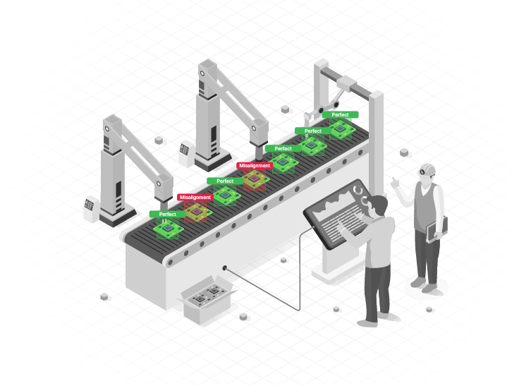
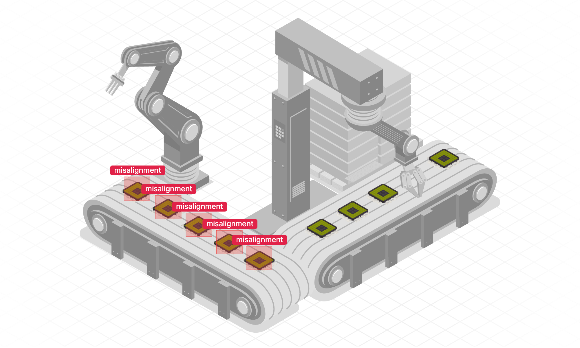
AI-powered AOI systems inspect PCBs used in semiconductor modules for opens, shorts, solder bridges, and misalignments.
Computer vision systems analyze plasma chamber visuals to predict etch completion with high accuracy, beyond time-based methods.
Real-time vision detects film streaks, particulate inclusions, and coating thickness inconsistencies in photoresist application.
Vision systems validate top-and-bottom die alignment and interconnect placement in PoP configurations before final assembly.

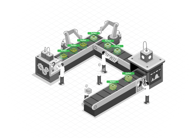
Gain full visibility into cleanroom operations with AI-driven insights across inspection, alignment, and defect control, helping reduce downtime and boost yield across wafer lots in any semiconductor fab facility.

Ensure sub-micron pattern fidelity, overlay accuracy, and surface uniformity with computer vision tools optimized for complex processes like lithography, CMP, and etching, ideal for custom semiconductor fabrication.

Minimize human exposure in hazardous cleanroom zones, detect thermal anomalies or manual intervention, and maintain compliance through real-time AI surveillance, especially in new or legacy semiconductor fabrication plants.

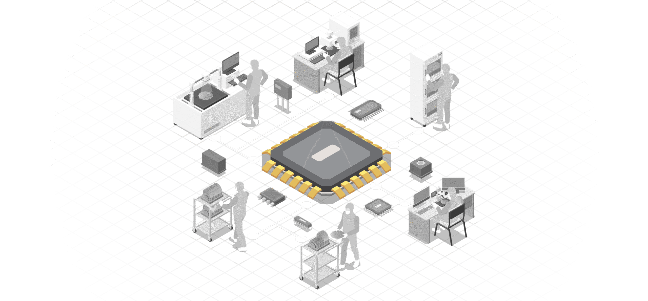
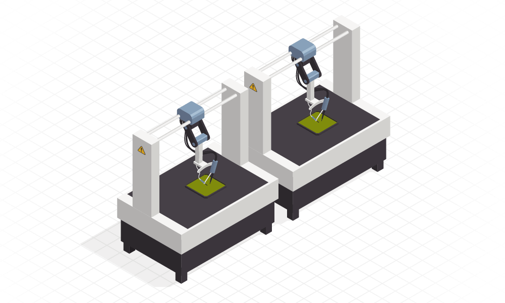
AI Vision systems engineered for ultra-clean, sub-micron environments in fabs, purpose-built for photomasks, wafers, packaging lines, and advanced nodes across global semiconductor companies.

Detects pattern defects, film inconsistencies, alignment errors, and overlay deviations, critical for modern IC fabrication process control.

Avoids rework by identifying defects early in the process, minimizing downtime, and maintaining a higher first-pass yield rate, across both legacy fabs and every new semiconductor plant.

Continuously monitors wafer movement, tool condition, and critical operations like etching and coating with real-time AI tracking, ideal for high-volume semiconductor fab workflows.

Reduces chemical waste, improves tool utilization, and supports predictive maintenance through actionable visual analytics in both advanced and standard fab facilities.

Limits human exposure through remote monitoring, reduces contamination risk, and detects manual errors that compromise process integrity.
Computer vision enables fast, accurate inspection at every stage, from photomask to packaging, by detecting defects invisible to the human eye. It ensures consistency, improves yield, and reduces manual inspection errors, all while keeping up with the scale of modern semiconductor fabrication demands.
AI vision doesn’t replace tools like SEM, it complements them by offering inline, real-time defect detection. It reduces the load on offline analysis, catches problems earlier, and speeds up process correction without disrupting throughput in your semiconductor manufacturing plant.
AI learns from historical data to detect subtle process drifts, misalignments, or surface issues before they become costly. With predictive alerts and feedback, semiconductor fabs can stabilize operations, reduce rework, and maintain consistent output.
Yes, AI vision systems are designed for sub-nanometer accuracy, making them suitable for EUV, FinFET, and advanced packaging. They adapt to complex geometries and maintain inspection reliability, even in next-gen IC fabrication processes.
Integration involves placing vision systems at key points, training models on your defect data, and connecting with your MES or tool controllers. It’s non-intrusive, fast to deploy, and starts delivering insights and alerts almost immediately, making it ideal for any semiconductor fab facility.
Stay updated with the trending and most impactful tech insights. Check out the expert analyses, real-world applications, and forward-thinking ideas that shape the future of AI Computer Vision and innovation.
Walk into a semiconductor fabrication plant in 2025 and you’ll see something that looks more like a science fiction set than a factory. Robots glide across spotless cleanrooms, wafers are carried through vacuum-sealed chambers, and machines whisper in precision rhythms. Each wafer that enters the fab is a canvas on which billions of transistors will […]

CEO & Co-founder
Every chip in your phone, your laptop, or even in a satellite, begins as a plain slice of silicon. But before that slice can become the heart of advanced electronics, it has to go through a series of complex processes. One of the least understood, yet most critical of these, is called Chemical Mechanical Planarization, […]
CEO & Co-founder
The story of the semiconductor industry is the story of human ambition to make things smaller, faster, and more powerful. We take this progress for granted when we buy a smartphone with a faster processor or a laptop with improved battery life, but behind these leaps lies an unforgiving pursuit of perfection at scales smaller […]
CEO & Co-founder