



















Certified information security and AI. Your Data secured and Private to you.
Talk with us
Ensure Perfect Boards Before Final Assembly. Automate Inspection. Assure Reliability.
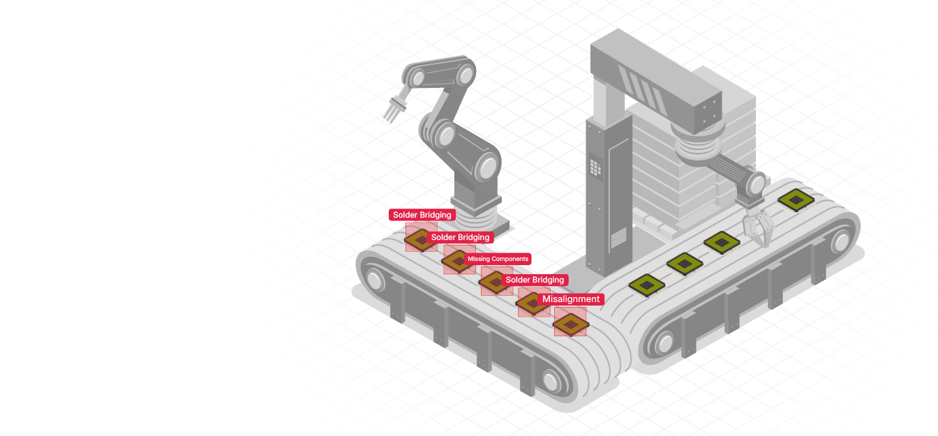
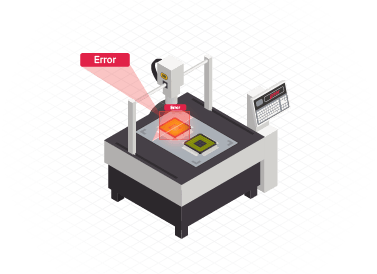
In semiconductor packaging, printed circuit boards (PCBs) form the structural and electrical base for advanced modules like SiPs (System-in-Package), PoP (Package-on-Package), and MCMs (Multi-Chip Modules). Faults in PCB assembly, like solder bridging, missing components, or misalignments, can introduce latent defects that pass undetected into critical applications.
AI-powered Automated Optical Inspection (AOI) systems scan each PCB for visual anomalies using high-speed cameras and deep learning models. These systems detect opens, shorts, solder joint irregularities, and missing or misplaced components, ensuring only fully functional modules proceed to final packaging or shipment.

Visual faults like cold solder, lifted leads, or hidden shorts can go undetected without automated inspection.

Human error increases under high volume and density, especially for fine-pitch BGA and SMT components.

Slight component rotation, tilt, or offset can cause functional failure post-reflow or during final testing.

Defects caught late in final test or burn-in increase cost of scrap or rework at the final stage.

Captures PCBs from multiple angles to assess placement, alignment, and solder quality in real-time.

Deep learning identifies cold joints, insufficient solder, bridging, and tombstoning with high accuracy.

Confirms correct part number, polarity, and presence using OCR and pattern-matching across densely populated PCBs.

Uses advanced light modeling or X-ray assisted AOI for partially hidden joints in high-density boards.
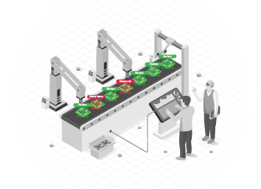

We begin by integrating the AOI unit between reflow oven exit and ICT/test stations. Conveyor speed, tray types, and PCB dimensions are mapped for optimized imaging cadence.

AOI hardware includes top, angled, and oblique-view cameras with adjustable lighting modules to eliminate reflections and shadows from solder joints.

Our team trains a defect model using annotated images from your specific board layouts, component placements, pad shapes, stencil types, and defect types.

Inspection results are streamed directly to your MES or line controller. Defective PCBs can be auto-routed to rework lanes, while analytics dashboards log recurring fault patterns by station or shift.
Stay updated with the trending and most impactful tech insights. Check out the expert analyses, real-world applications, and forward-thinking ideas that shape the future of AI Computer Vision and innovation.
Three months after the incident, the assessor sits across from Meera, the operations manager, and slides a form over the desk. She is ready for questions about helmets, about whether the supervisor was present, about protocol. He asks none of them. He asks one thing instead: show me the footage. Meera’s yard runs safety well. […]

CEO & Co-founder

Deepak runs operations at a mid-size terminal, and one number has bothered him for a month. Two ship-to-shore cranes, side by side. Same model, same year, same maintenance schedule. Crews rotate between them every shift. One averages 22 moves an hour. The other averages 30. He sends a maintenance team over the slow one. They […]
CEO & Co-founder
Pravin has run the empty depot for nine years, and he will tell you he knows every box in it. Then he walks you to the far corner, points at a container furred with dust, a small spider web in the corner casting, and goes quiet. It came in months ago. Nobody remembers the booking. […]
CEO & Co-founder
