
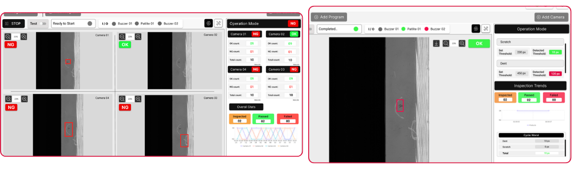
Customer
A global screen inspector and repair company.
Project Details
- Duration: 5 Months
Technologies:
- Tensorflow
- Deep Learning
- AI Vision
- OpenCV
- Python
A global screen inspector and repair company.
Technologies:
Accuracy
Reduction in time for Manual Verification


Stay updated with the trending and most impactful tech insights. Check out the expert analyses, real-world applications, and forward-thinking ideas that shape the future of AI Computer Vision and innovation.

Three months after the incident, the assessor sits across from Meera, the operations manager, and slides a form over the desk. She is ready for questions about helmets, about whether the supervisor was present, about protocol. He asks none of them. He asks one thing instead: show me the footage. Meera’s yard runs safety well. […]

CEO & Co-founder

Deepak runs operations at a mid-size terminal, and one number has bothered him for a month. Two ship-to-shore cranes, side by side. Same model, same year, same maintenance schedule. Crews rotate between them every shift. One averages 22 moves an hour. The other averages 30. He sends a maintenance team over the slow one. They […]
CEO & Co-founder
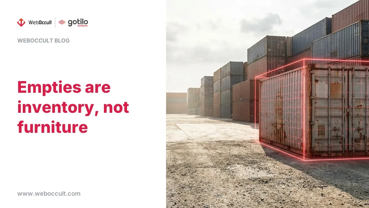
Pravin has run the empty depot for nine years, and he will tell you he knows every box in it. Then he walks you to the far corner, points at a container furred with dust, a small spider web in the corner casting, and goes quiet. It came in months ago. Nobody remembers the booking. […]
CEO & Co-founder
