Surface Defect Detection
Detect micro-defects, ensure quality, and reduce wastage with precision AI vision.
Detect micro-defects, ensure quality, and reduce wastage with precision AI vision.
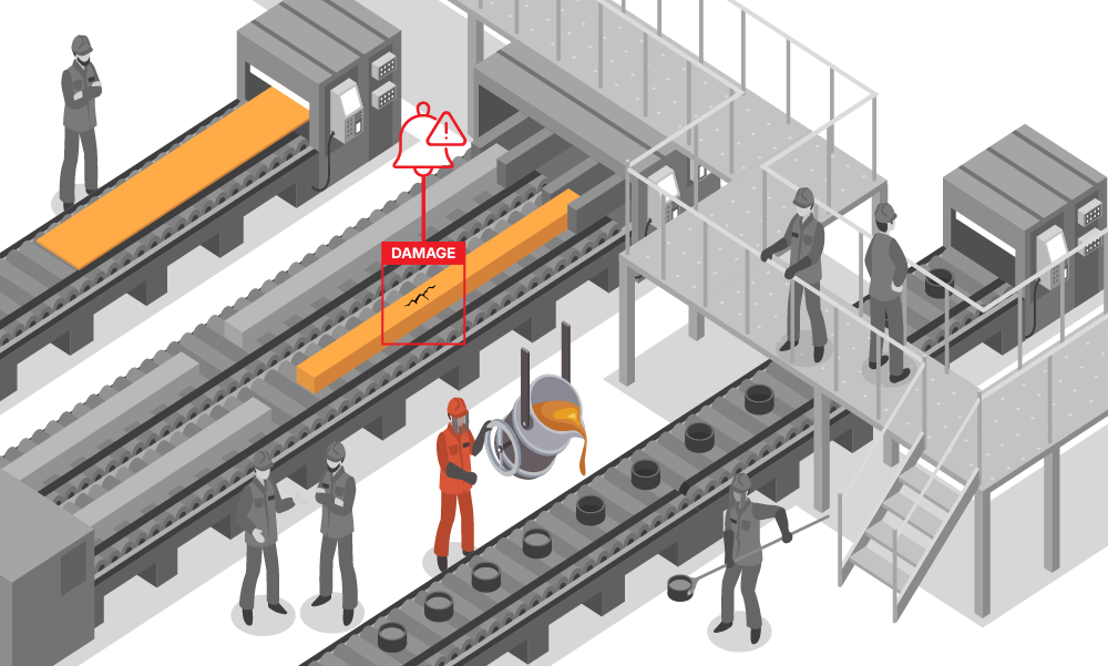
Surface Defect Detection powered by AI computer vision transforms quality control in the steel industry. It automatically scans hot and cold rolled surfaces to identify cracks, scale, pinholes, laminations, dents, or scratches in real time, well before they move further in the process.

Surface flaws like pinholes, cracks, or inclusions often go unnoticed during visual inspections, leading to high rejection rates later.

Human-led surface checks are inconsistent, prone to fatigue, and may vary across shifts or lighting conditions.

Defects are often caught too late, after finishing or packaging, wasting time, effort, and material.

Manual checks or re-inspections cause bottlenecks, slowing down continuous steel production.

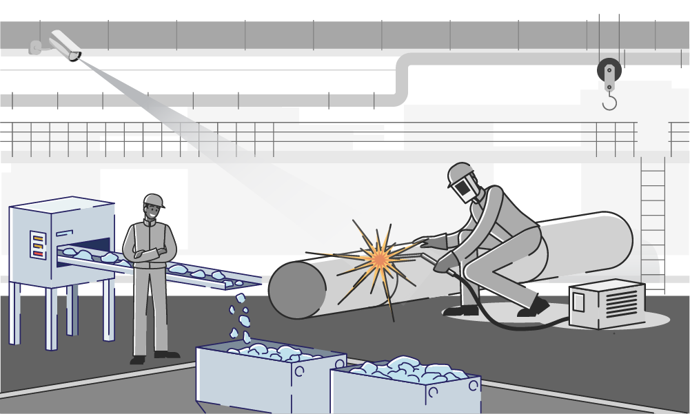
Captures ultra-clear visuals of steel surfaces to detect even the smallest of irregularities in real time.

Deep learning models trained to identify, categorize, and prioritize various surface defects instantly.

Operators receive instant notifications with defect type, location, and severity, enabling fast action.

Easily deployable on existing production lines without disrupting the process or requiring infrastructure overhaul.
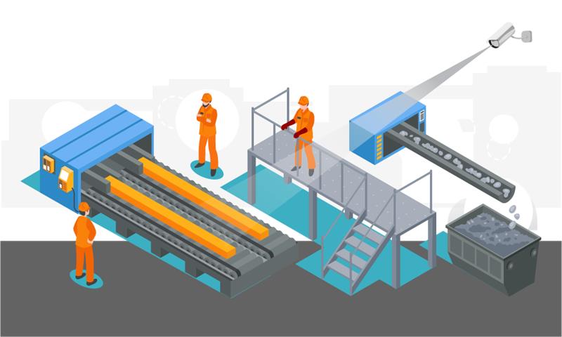

Before cameras are placed, our team works closely with your QA and production heads to identify key defect-prone zones in your process, from roughing to finishing stages.

Unlike container OCR or standard object detection, steel surfaces require adaptive camera calibration to handle hot metal glare, scale, and high-speed movement. We tune exposure, frame rate, and sensor placement accordingly.

Using your past defect data (images, logs), we build a steel-grade-specific model that understands localized terminology and defect variations, whether its centerline cracks or transverse marks.

The model is installed alongside your HMI or MES systems. We enable shift-level visibility, automatic tagging for rework, and live dashboards. Testing is done under real heat-load, ambient light, and line-speed conditions.
Stay updated with the trending and most impactful tech insights. Check out the expert analyses, real-world applications, and forward-thinking ideas that shape the future of AI Computer Vision and innovation.
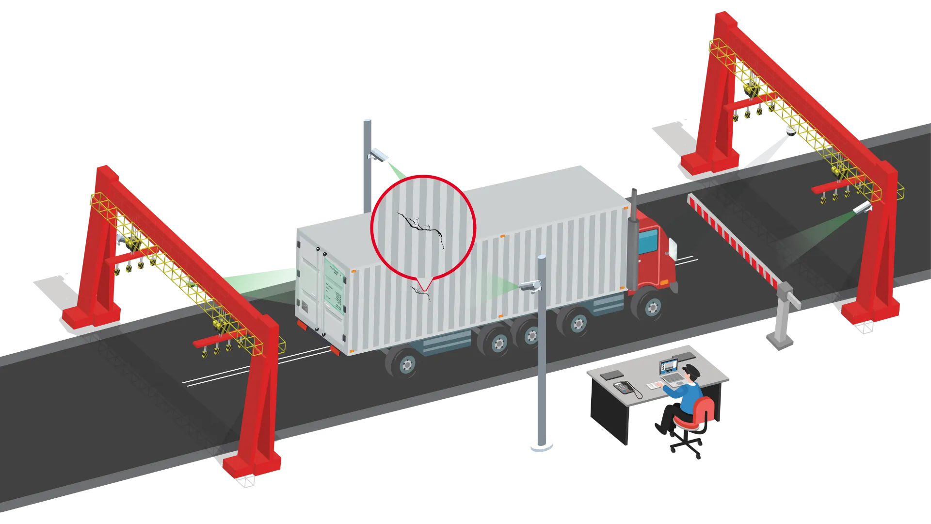
At midnight, a high value shipment enters a regional logistics hub. By morning, the factory waited for those parts to halt production. The system shows the shipment as “received.” The yard team insists it was unloaded. The transporter says it left in perfect condition. No one is lying. No one can prove anything either. This […]

CEO & Co-founder
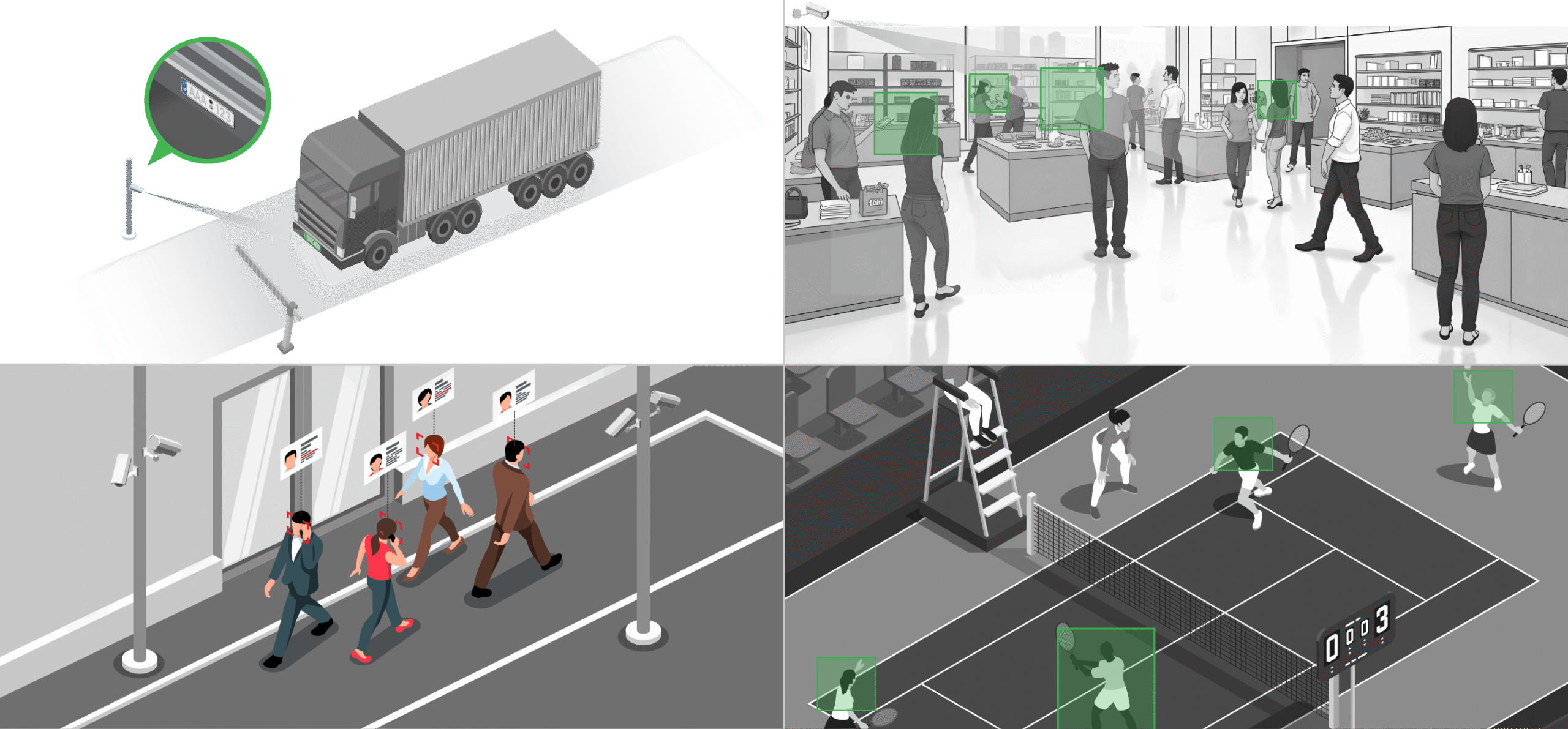
What ties these everyday moments together? It all looks connected… until you notice the pattern! Keep reading to know what? A truck entering a manufacturing campus. Crowds moving through a large exhibition hall. Containers rolling past a busy port gate. Players training across multiple tennis courts. Employees moving in and out of shared office spaces. […]
CEO & Co-founder
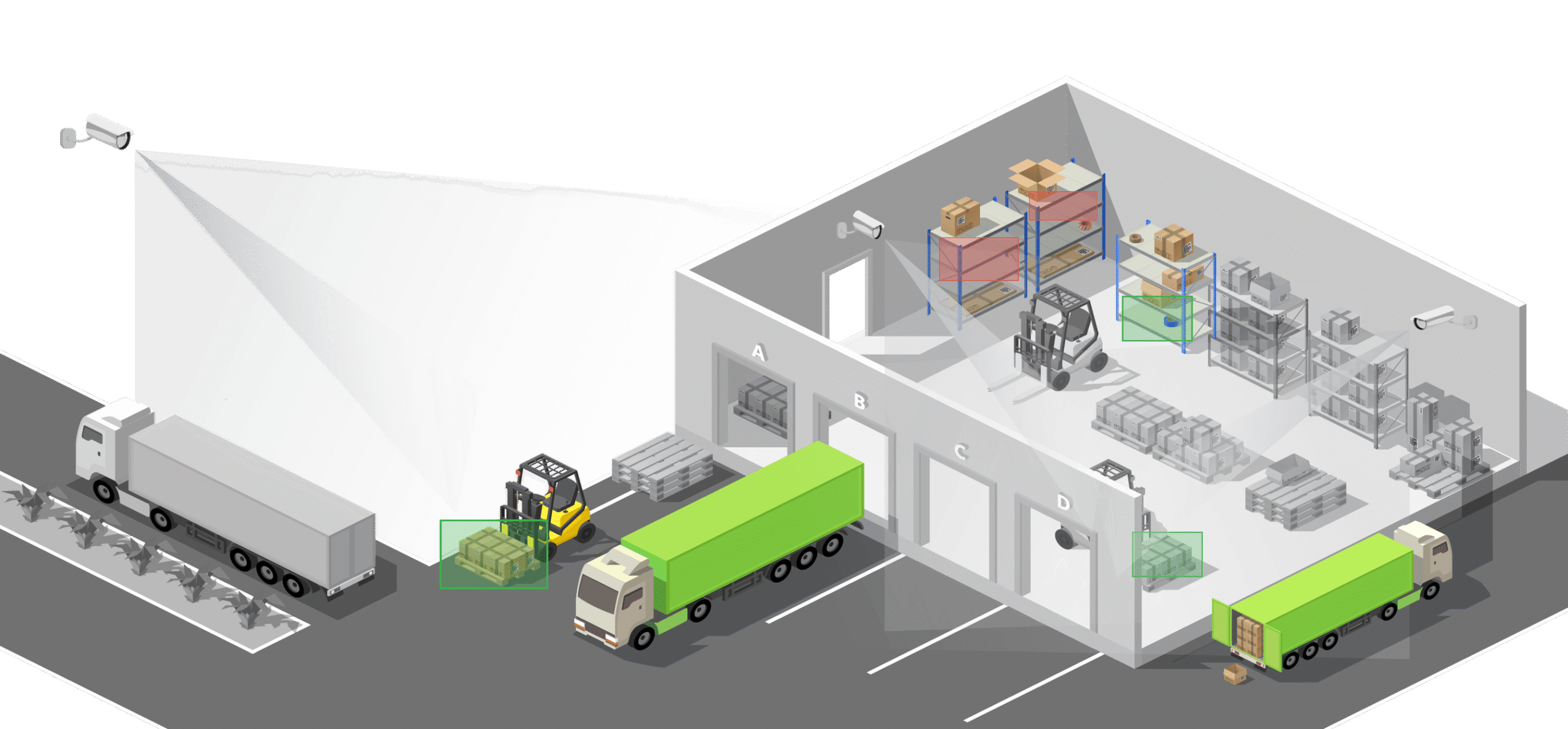
7:45AM at a busy automotive parts manufacturer. A delivery truck arrived at the dock. Usually, supervisors would take 10 minutes to scan paperwork. They’d also be keying in data. Instead, a camera quietly recorded the container ID, logged upon its arrival. And it tagged the shipment to a specific production line. All without a single […]
CEO & Co-founder
