Resist Coating Uniformity & Defect Monitoring
Perfect the Coat. Eliminate Contamination. Ensure Photolithography Precision.
Perfect the Coat. Eliminate Contamination. Ensure Photolithography Precision.
Photoresist coating is the first critical step in wafer patterning, any variation in film thickness, streaks, or contamination can cause pattern distortion or complete lithography failure. Yet, traditional inline checks or manual inspections often miss these subtle but fatal errors.
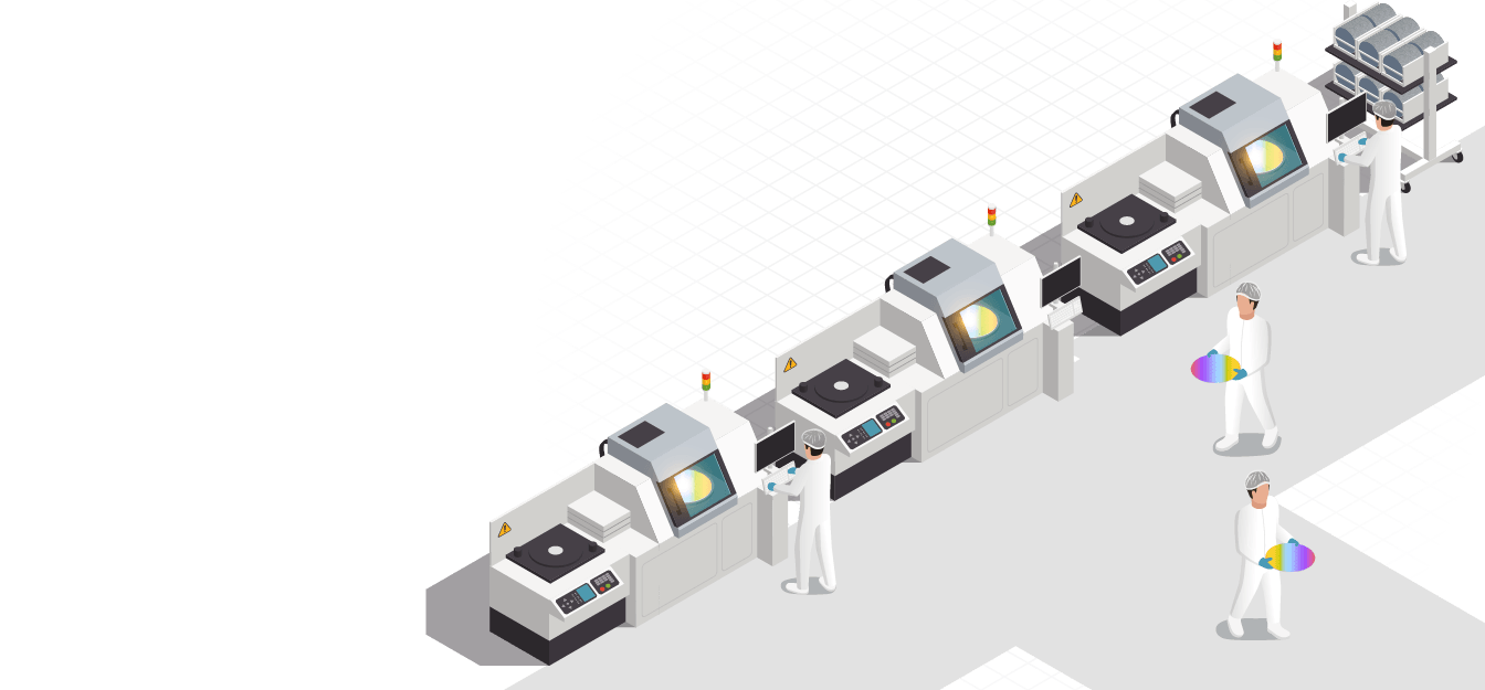
AI-powered Resist Coating Uniformity & Defect Monitoring uses computer vision to continuously inspect resist film application in real-time. It tracks film consistency, detects defects like bubbles, streaks, and particles, and identifies non-uniform thickness across the wafer, before the wafer reaches the exposure tool.

Variations across wafer radius or from batch-to-batch can result in uneven exposure or resist development.

Bubbles, streaks, or particles are difficult to catch without consistent high-resolution inspection.

Poor edge bead removal (EBR) or aging resist causes contamination at the wafer edge, reducing usable area.

Defects are often discovered only after exposure or development, too late for correction.

High-speed cameras scan coated wafers for surface anomalies and coating consistency before exposure.

Visual data is processed to detect microns of variation across wafer zones and flag abnormal patterns.

Identifies EBR failures, air bubble entrapments, and inconsistent spin profiles that can compromise quality.

Automatically stops defective wafers from progressing and recommends rework, saving exposure tool cycles.


We begin by identifying the optimal inspection point, typically between the spin coater and EBR or before bake, to ensure full visual access before exposure.

Camera and lighting systems are tuned to work across multiple resist chemistries and coating speeds, with configurable profiles for each product line.

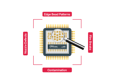
Our models are trained using historical coated wafer data, including edge bead patterns, film breaks, nozzle defects, and particulate contamination.

The inspection system sends “pass,” “hold,” or “re-coat” commands directly to your MES system, while simultaneously logging heatmaps and coating stats per wafer ID for traceability.
Stay updated with the trending and most impactful tech insights. Check out the expert analyses, real-world applications, and forward-thinking ideas that shape the future of AI Computer Vision and innovation.
Busy container terminal at 6 AM. Trucks queuing at the gate, vessels berthing, yard equipment moving in every direction, and somewhere in the middle of all that organized chaos, a gate clerk squinting at a container number that’s half-obscured by road grime, trying to type it correctly into a system that will not forgive a […]

CEO & Co-founder

There’s a strawberry sitting in a warehouse in a port somewhere in Europe right now. It was picked three days ago. And if someone doesn’t know exactly what temperature it’s been kept at for the last 72 hours, that strawberry, and about 40,000 others just like it, might be quietly rotting. Nobody talks about that […]
CEO & Co-founder
At midnight, a high value shipment enters a regional logistics hub. By morning, the factory waited for those parts to halt production. The system shows the shipment as “received.” The yard team insists it was unloaded. The transporter says it left in perfect condition. No one is lying. No one can prove anything either. This […]
CEO & Co-founder
