PHOTOMASK DEFECT INSPECTION
Catch Sub-Micron Errors. Preserve Pattern Integrity. Enhance Yield at the First Step.
Catch Sub-Micron Errors. Preserve Pattern Integrity. Enhance Yield at the First Step.
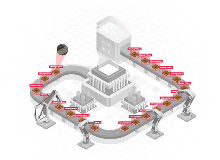
Photomasks are the blueprint of semiconductor manufacturing, and even the tiniest imperfection can lead to costly wafer defects across thousands of chips. Traditional manual and rule-based inspections are no longer viable for today’s advanced nodes. AI-powered Photomask Defect Inspection leverages ultra-high-resolution imaging combined with deep learning to detect sub-micron flaws like missing patterns, particles, scratches, or deformation, before they are replicated during lithography.

Human inspection or traditional rule-based systems struggle to catch nano-scale particles or structural flaws on masks.

High rejection rate of usable masks due to overly sensitive or static threshold systems.

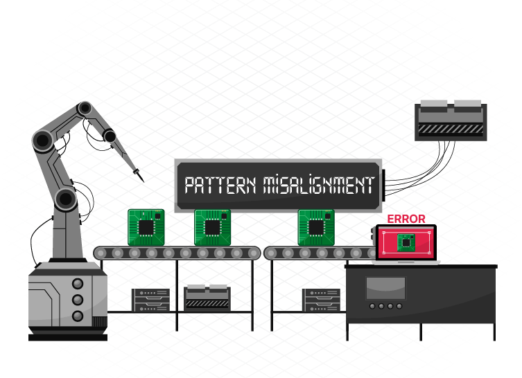
Even when defects are detected, they are often not correctly categorized, slowing down root cause analysis.

Long inspection cycles and repeated mask validations delay exposure steps and increase cycle times.

AI models trained on vast defect datasets to detect and differentiate critical vs. non-critical anomalies.

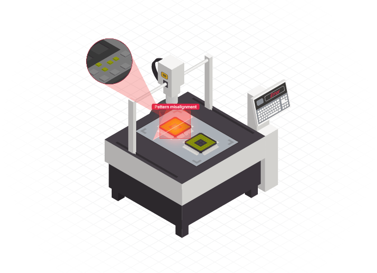
Micron and sub-micron precision imaging using specialized optics to catch the smallest pattern inconsistencies.

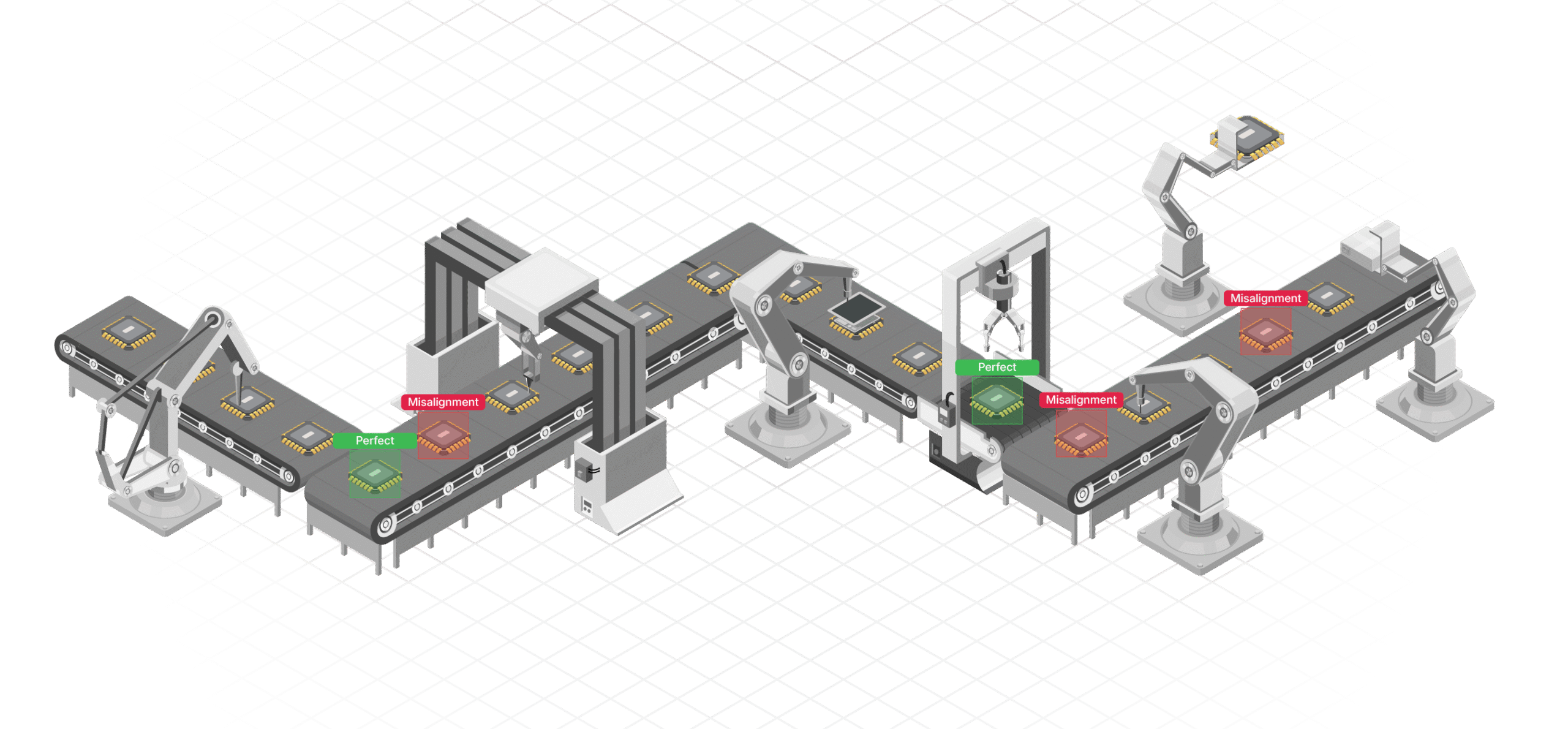
Classifies defect types (particles, scratches, edge defects, missing lines) and ranks them by severity and location.

Compares actual mask pattern with design files (GDSII) for pixel-level mismatch detection.

The system begins by ingesting GDSII design files of the intended mask layout. These files are used to create pixel-level reference patterns for comparison.

Specialized imaging systems are calibrated to achieve ultra-high resolution (sub-100nm) and correct for lens distortion, lighting uniformity, and reflectivity of mask surfaces.

Historical mask defect data, including particle types, line breaks, and haze, is used to train a defect classification model that distinguishes real issues from noise or permissible variations.

Captured images are analyzed frame-by-frame using AI models, and inspection results are displayed on an intuitive dashboard. Critical defects are flagged for review, while acceptable ones are auto-classified, reducing manual load.
Stay updated with the trending and most impactful tech insights. Check out the expert analyses, real-world applications, and forward-thinking ideas that shape the future of AI Computer Vision and innovation.
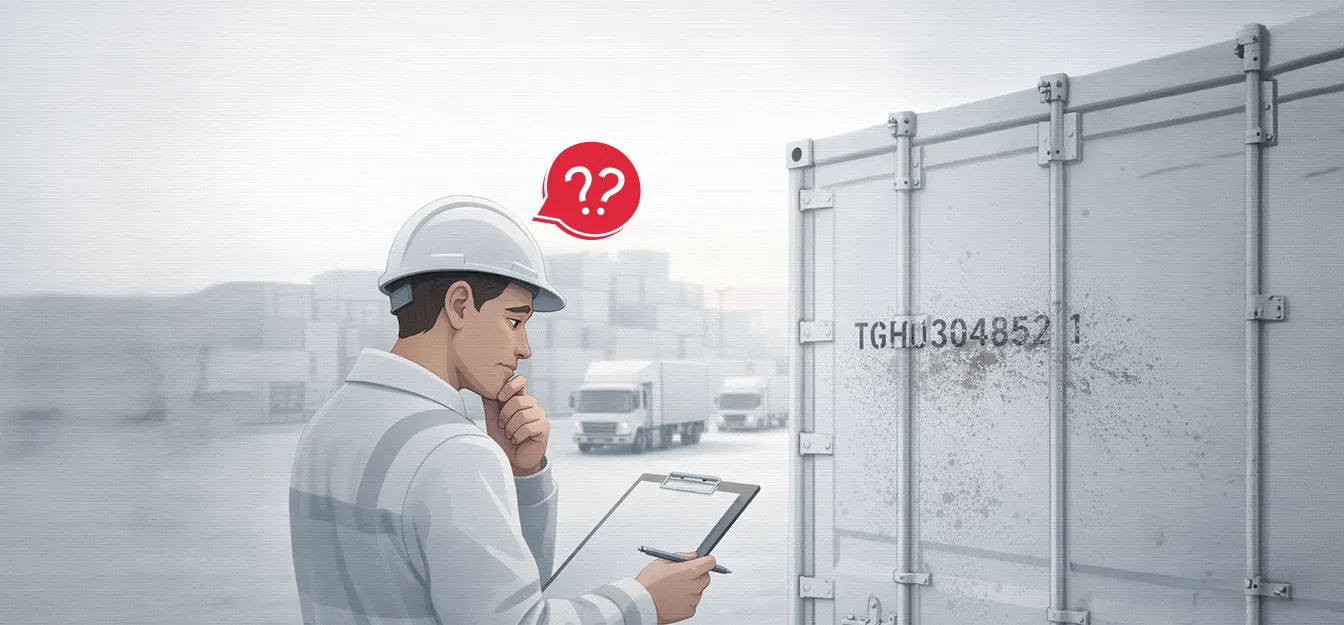
Busy container terminal at 6 AM. Trucks queuing at the gate, vessels berthing, yard equipment moving in every direction, and somewhere in the middle of all that organized chaos, a gate clerk squinting at a container number that’s half-obscured by road grime, trying to type it correctly into a system that will not forgive a […]

CEO & Co-founder
There’s a strawberry sitting in a warehouse in a port somewhere in Europe right now. It was picked three days ago. And if someone doesn’t know exactly what temperature it’s been kept at for the last 72 hours, that strawberry, and about 40,000 others just like it, might be quietly rotting. Nobody talks about that […]
CEO & Co-founder
At midnight, a high value shipment enters a regional logistics hub. By morning, the factory waited for those parts to halt production. The system shows the shipment as “received.” The yard team insists it was unloaded. The transporter says it left in perfect condition. No one is lying. No one can prove anything either. This […]
CEO & Co-founder
