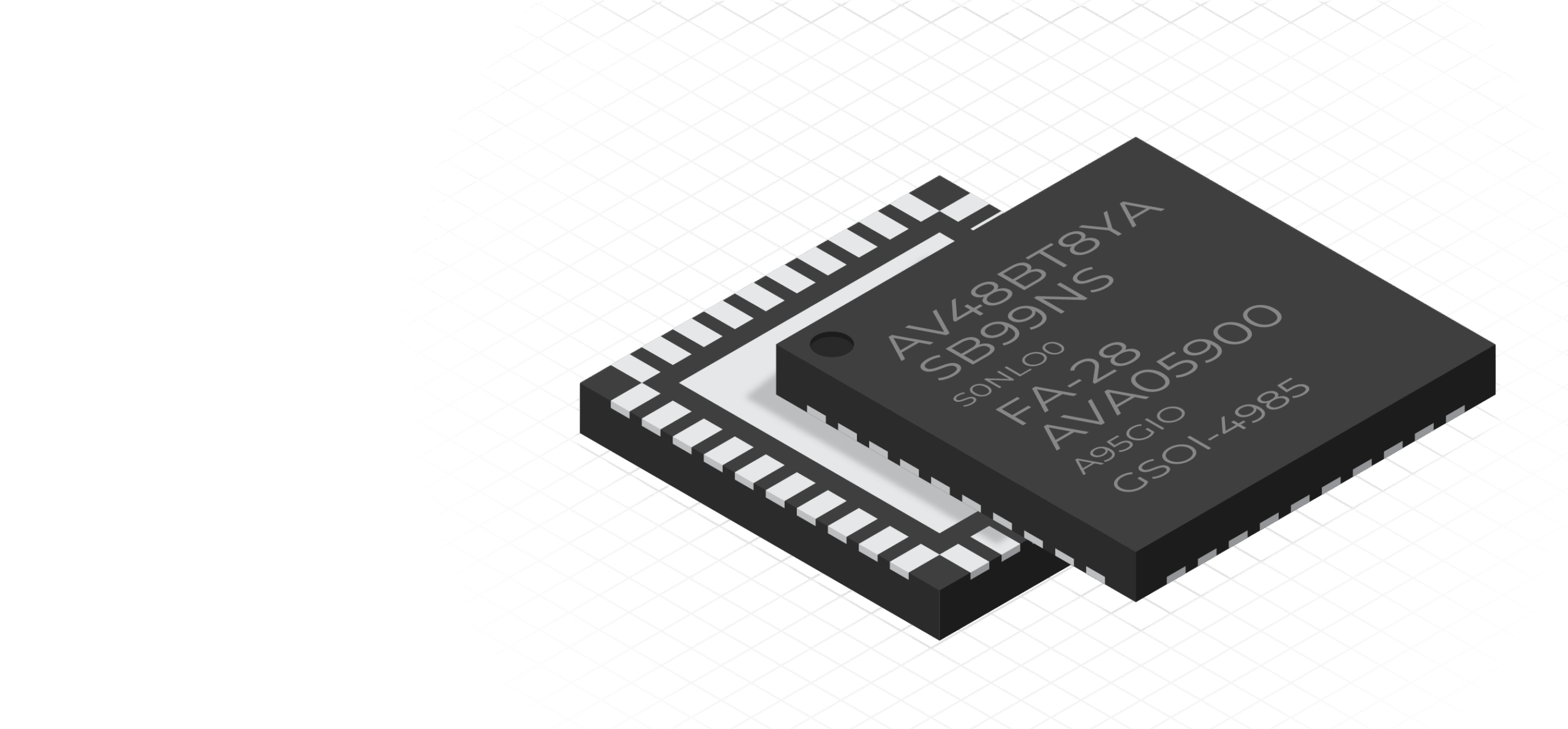
Package-On-Package (PoP) Assembly Validation
Verify Every Layer. Validate Every Connection. Stack with Confidence.
Verify Every Layer. Validate Every Connection. Stack with Confidence.
Package-on-Package (PoP) is central to high-density mobile and consumer electronics, allowing multiple dies to be vertically integrated. But even the slightest vertical misalignment, offset solder balls, or warpage can lead to latent electrical failures that are hard to catch during final testing.
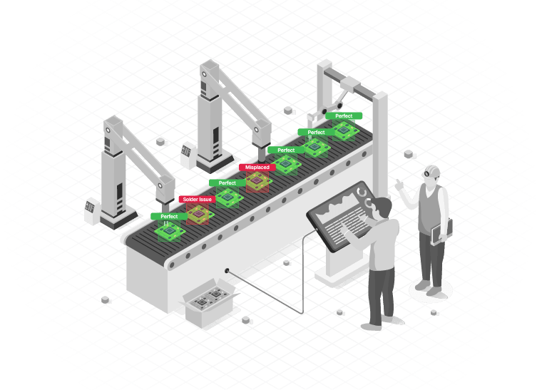
AI-powered PoP Assembly Validation uses advanced computer vision systems to inspect stacked die alignment, verify solder ball contact, and confirm Z-axis symmetry before the final reflow step. These inspections ensure mechanical integrity, electrical continuity, and proper height uniformity across units.

Even a slight X-Y or rotational offset between the top and bottom packages can compromise interconnects.

Incomplete, tilted, or shifted ball contacts often go undetected until after reflow or in final test.

Mechanical stress during stacking can deform the top die, leading to contact failure or packaging instability.

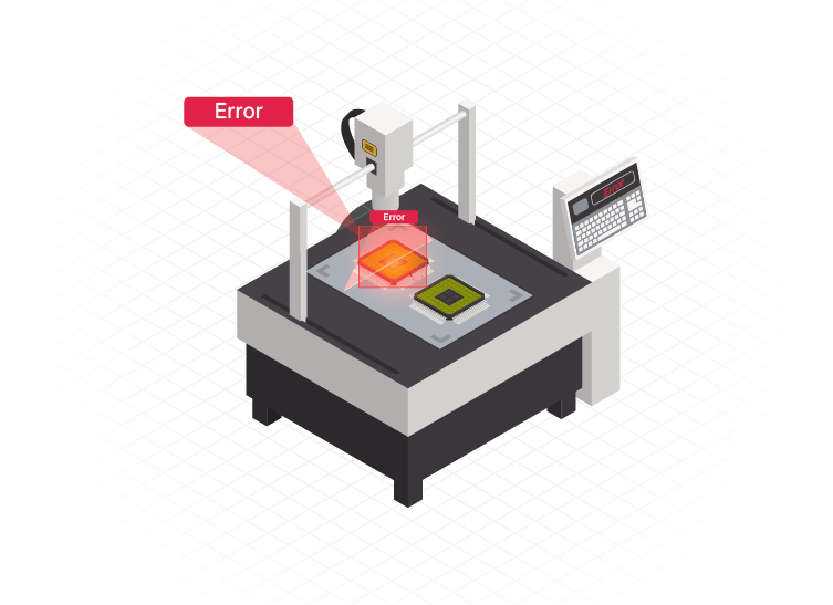
Manual or 2D inspection can’t detect vertical skew or stack height irregularities, which are critical in PoP.

Captures vertical alignment, height, and planarity using stereo or laser triangulation imaging.

AI verifies the concentricity and location of each solder ball against landing pads across layers.

Detects bowing, tilt, or sagging in the top die pre-reflow, reducing latent defect risks.

Assigns assembly units into pass/fail/rework bins based on deviation from set tolerances.

We begin by identifying the optimal point for PoP validation, usually after top package placement but before reflow. Fixture mapping includes robotic arm paths and hold time.

Combining top-down visual inspection with structured light or laser triangulation systems, we capture full X-Y-Z data of the stacked unit in motion.

Training includes past examples of vertical tilt, side-shift, solder ball misalignment, and package deformation, enabling the model to distinguish between acceptable and critical faults.

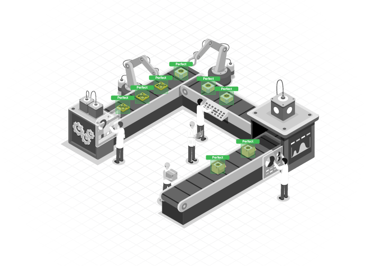
Each inspected unit is tagged with height maps and alignment metrics. Results are pushed into the MES for traceability, and robotic sorters are triggered to route the unit based on tolerance bins (pass/rework/fail).
Stay updated with the trending and most impactful tech insights. Check out the expert analyses, real-world applications, and forward-thinking ideas that shape the future of AI Computer Vision and innovation.
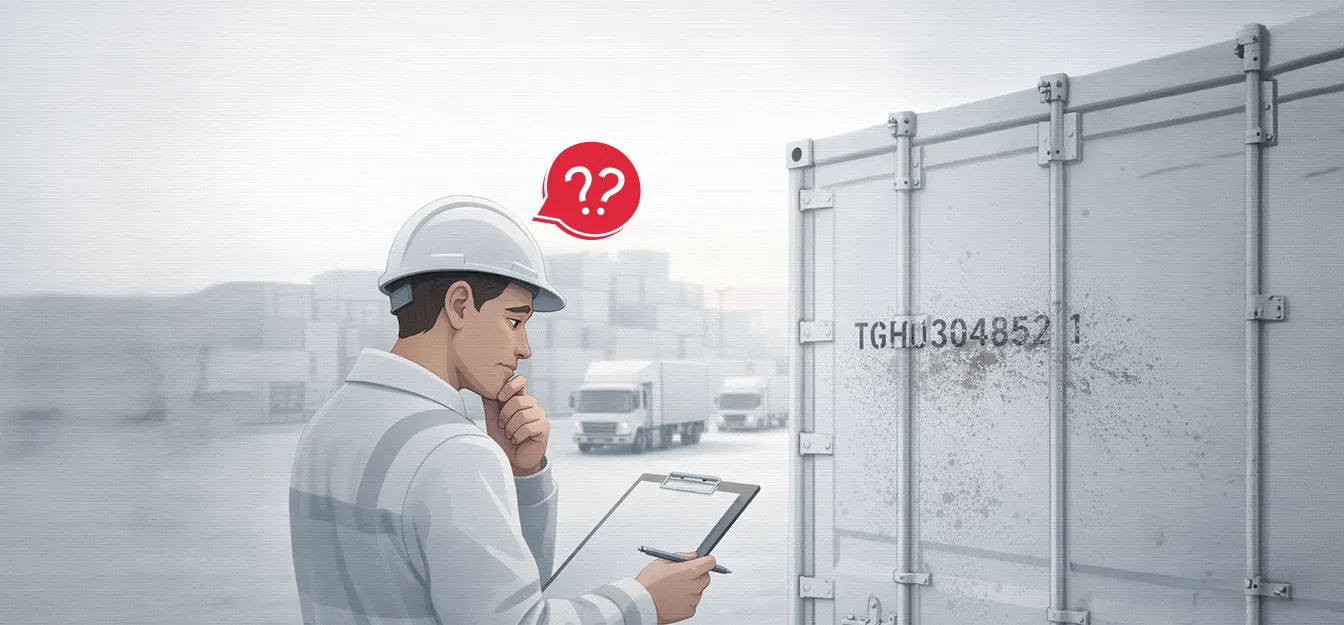
Busy container terminal at 6 AM. Trucks queuing at the gate, vessels berthing, yard equipment moving in every direction, and somewhere in the middle of all that organized chaos, a gate clerk squinting at a container number that’s half-obscured by road grime, trying to type it correctly into a system that will not forgive a […]

CEO & Co-founder
There’s a strawberry sitting in a warehouse in a port somewhere in Europe right now. It was picked three days ago. And if someone doesn’t know exactly what temperature it’s been kept at for the last 72 hours, that strawberry, and about 40,000 others just like it, might be quietly rotting. Nobody talks about that […]
CEO & Co-founder
At midnight, a high value shipment enters a regional logistics hub. By morning, the factory waited for those parts to halt production. The system shows the shipment as “received.” The yard team insists it was unloaded. The transporter says it left in perfect condition. No one is lying. No one can prove anything either. This […]
CEO & Co-founder
