Lead Frame And Substrate Inspection
Inspect Before You Bond. Prevent Failure Before Assembly.

Inspect Before You Bond. Prevent Failure Before Assembly.
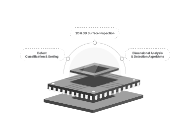
Lead frames and substrates form the physical base for semiconductor packages, any warpage, contamination, or dimensional fault at this level can cause bonding issues, electrical shorts, or total package failure. Manual inspection is inconsistent, and traditional 2D tools often miss warpage or multilayer misalignment. AI-powered Lead Frame and Substrate Inspection uses advanced 2D/3D computer vision to detect surface defects, warpage, and structural misalignment before die attach or wire bonding. With micron-level resolution and intelligent classification, the system ensures only flawless frames proceed to the next stage.

Scratches, dents, or oxidation on the lead frame surface may go undetected in visual checks, leading to bonding failure.

Substrate thickness, paddle depth, or pad spacing variations cause die misplacement or electrical mismatch.

Mechanical warpage due to improper storage or handling can cause poor die attach, especially in multi-layer substrates.

Human error and subjective judgment reduce reliability and throughput under high-volume demands.

Captures surface irregularities, corrosion, scratches, and dents using high-resolution visual and depth scanning.

Measures pad pitch, bond fingers, paddle flatness, and outline dimensions against golden specs.

Uses machine vision with 3D reconstruction to detect bending or structural warpage in substrates and frames.

Automatically classifies defects and routes defective units to rework bins or rejects them, no operator input needed.
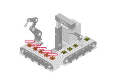

We begin by mapping the inspection point between cleaning and die attach stages, integrating the system with your substrate loader/unloader and frame handler.

Combining area-scan cameras and laser triangulation sensors, we enable full-surface and height-map acquisition for each lead frame or substrate in motion.

Our AI model is trained on real-world defect libraries from your past rejects, scratches, oxide marks, pad shifts, to achieve context-specific classification.

Inspection outcomes are sent to the MES (Manufacturing Execution System) in real time, triggering robotic sorters or binning logic to separate units by defect class or reworkability.
Stay updated with the trending and most impactful tech insights. Check out the expert analyses, real-world applications, and forward-thinking ideas that shape the future of AI Computer Vision and innovation.

Busy container terminal at 6 AM. Trucks queuing at the gate, vessels berthing, yard equipment moving in every direction, and somewhere in the middle of all that organized chaos, a gate clerk squinting at a container number that’s half-obscured by road grime, trying to type it correctly into a system that will not forgive a […]

CEO & Co-founder

There’s a strawberry sitting in a warehouse in a port somewhere in Europe right now. It was picked three days ago. And if someone doesn’t know exactly what temperature it’s been kept at for the last 72 hours, that strawberry, and about 40,000 others just like it, might be quietly rotting. Nobody talks about that […]
CEO & Co-founder
At midnight, a high value shipment enters a regional logistics hub. By morning, the factory waited for those parts to halt production. The system shows the shipment as “received.” The yard team insists it was unloaded. The transporter says it left in perfect condition. No one is lying. No one can prove anything either. This […]
CEO & Co-founder
