HOT METAL TEMPERATURE VALIDATION
Ensure thermal accuracy. Prevent overheating. Maintain metallurgical precision in every pour.
Ensure thermal accuracy. Prevent overheating. Maintain metallurgical precision in every pour.
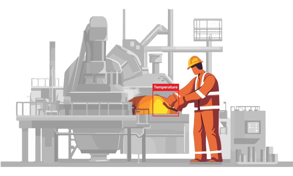
In the steel industry, even a few degrees can determine the success or failure of casting, rolling, or quenching. Manual temperature checks using handheld pyrometers or spot sensors are often delayed, inaccurate, or dangerously close to molten zones.Hot Metal Temperature Validation uses non-contact thermal imaging and AI analysis to provide continuous, real-time monitoring of molten metal and hot surfaces, ensuring exact thermal thresholds are maintained at each critical step, from ladle to line.

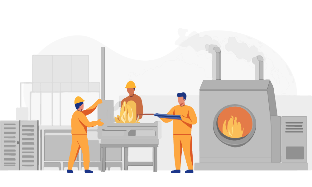
Handheld devices offer point readings that dont reflect true thermal spread or gradient.

Close-proximity measurements expose workers to extreme heat and radiant zones.

Failure to maintain optimal temperatures leads to poor grain structure or unwanted defects.

Temperature anomalies are often detected too late, after casting or forming errors have occurred.

Monitors temperature across entire metal surfaces using AI-enabled thermal cameras.

Alerts operators instantly when metal temperatures move beyond safe ranges.

Provides heat distribution maps to detect hotspots, cold zones, and uneven thermal flows.

Syncs with casting or rolling controls to auto-adjust feed rates or cooling cycles.

We begin by identifying key stages where temperature accuracy is essential, such as ladle pouring, tundish levels, rolling exit, or pre-quench zones.

Thermal cameras are selected and calibrated for extreme heat ranges (800°C 1650°C) and placed at safe, shielded observation points using industrial-grade enclosures.

AI models are trained on visual + thermal data to correlate metal color, glow, and behavior with accurate temperature bands across steel grades and process variations.

Live thermal maps and status alerts are integrated with the control room interface. Auto-alerts are triggered for overheating, heat loss, or uneven flow, enabling timely intervention.
Stay updated with the trending and most impactful tech insights. Check out the expert analyses, real-world applications, and forward-thinking ideas that shape the future of AI Computer Vision and innovation.
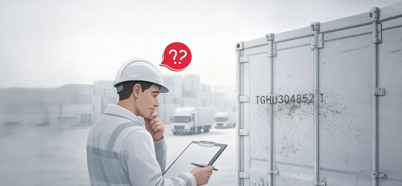
Busy container terminal at 6 AM. Trucks queuing at the gate, vessels berthing, yard equipment moving in every direction, and somewhere in the middle of all that organized chaos, a gate clerk squinting at a container number that’s half-obscured by road grime, trying to type it correctly into a system that will not forgive a […]

CEO & Co-founder
There’s a strawberry sitting in a warehouse in a port somewhere in Europe right now. It was picked three days ago. And if someone doesn’t know exactly what temperature it’s been kept at for the last 72 hours, that strawberry, and about 40,000 others just like it, might be quietly rotting. Nobody talks about that […]
CEO & Co-founder
At midnight, a high value shipment enters a regional logistics hub. By morning, the factory waited for those parts to halt production. The system shows the shipment as “received.” The yard team insists it was unloaded. The transporter says it left in perfect condition. No one is lying. No one can prove anything either. This […]
CEO & Co-founder
