CMP Quality Monitoring
Perfect the Planarity. Catch Surface Irregularities Before They Cost You Yield.
Perfect the Planarity. Catch Surface Irregularities Before They Cost You Yield.
Chemical Mechanical Planarization (CMP) is critical for achieving flat surfaces before lithography and metalization layers, but it’s also one of the most defect-prone processes in semiconductor fabrication. Microscopic erosion, dishing, scratches, and thickness variations can easily go undetected until later stages, causing metal bridging, poor pattern fidelity, and electrical faults.
AI-powered CMP Quality Monitoring systems use real-time computer vision and surface profiling to inspect wafers for planarity issues, pattern distortions, and mechanical damage, before wafers exit the CMP tool.

Surface depressions or raised areas often escape detection using static metrology tools.

By the time defects are caught, wafers have already moved forward, resulting in batch-level loss.

Traditional CMP lacks intelligent automation for adjusting pad pressure or slurry flow in real time.

Edge vs. center planarity variations often go undiagnosed without full-field visual inspection.

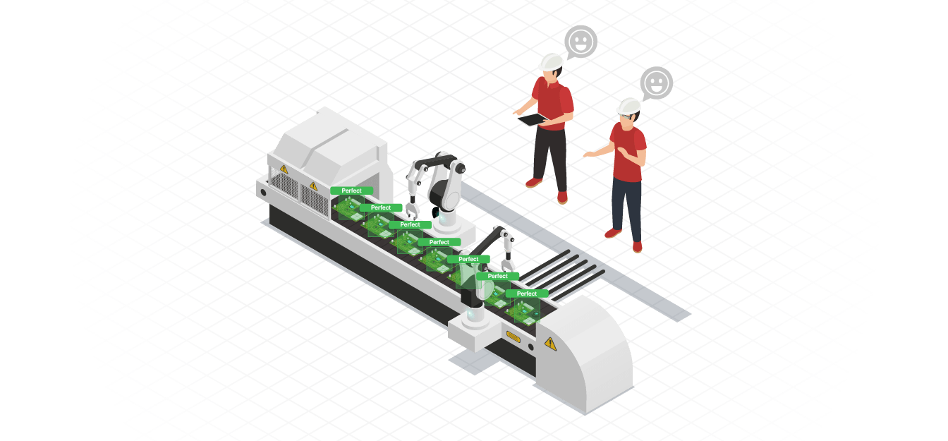
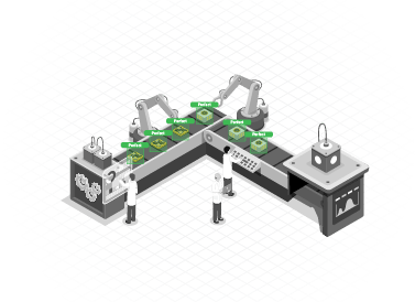
Vision systems detect topography variations like dishing, erosion, and micro-scratches as wafers exit the platen.

Full-wafer visual analysis to ensure uniform thickness across all regions.

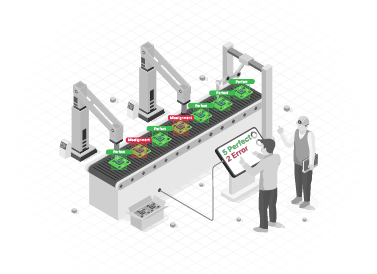
AI detects and classifies CMP-related defects using training data, reducing false positives.

Detects trends in pad wear or slurry issues and feeds data back to adjust process settings.

We begin by auditing your specific CMP tools, single or double platen, and defining inspection points for incoming and outgoing wafers.

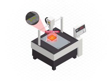
High-speed line-scan or area-scan cameras are calibrated for low reflectivity surfaces, mounted above wafer exit conveyors with optical flattening filters to reduce glare.

AI models are trained using thousands of annotated wafer images to recognize surface artifacts like microscratches, pad marks, and planar deviations with high accuracy.

The system is integrated directly into the CMP tool’s output lane or post-clean module, providing instant alerts for abnormal surface profiles and enabling dynamic process correction without production delay.
Stay updated with the trending and most impactful tech insights. Check out the expert analyses, real-world applications, and forward-thinking ideas that shape the future of AI Computer Vision and innovation.

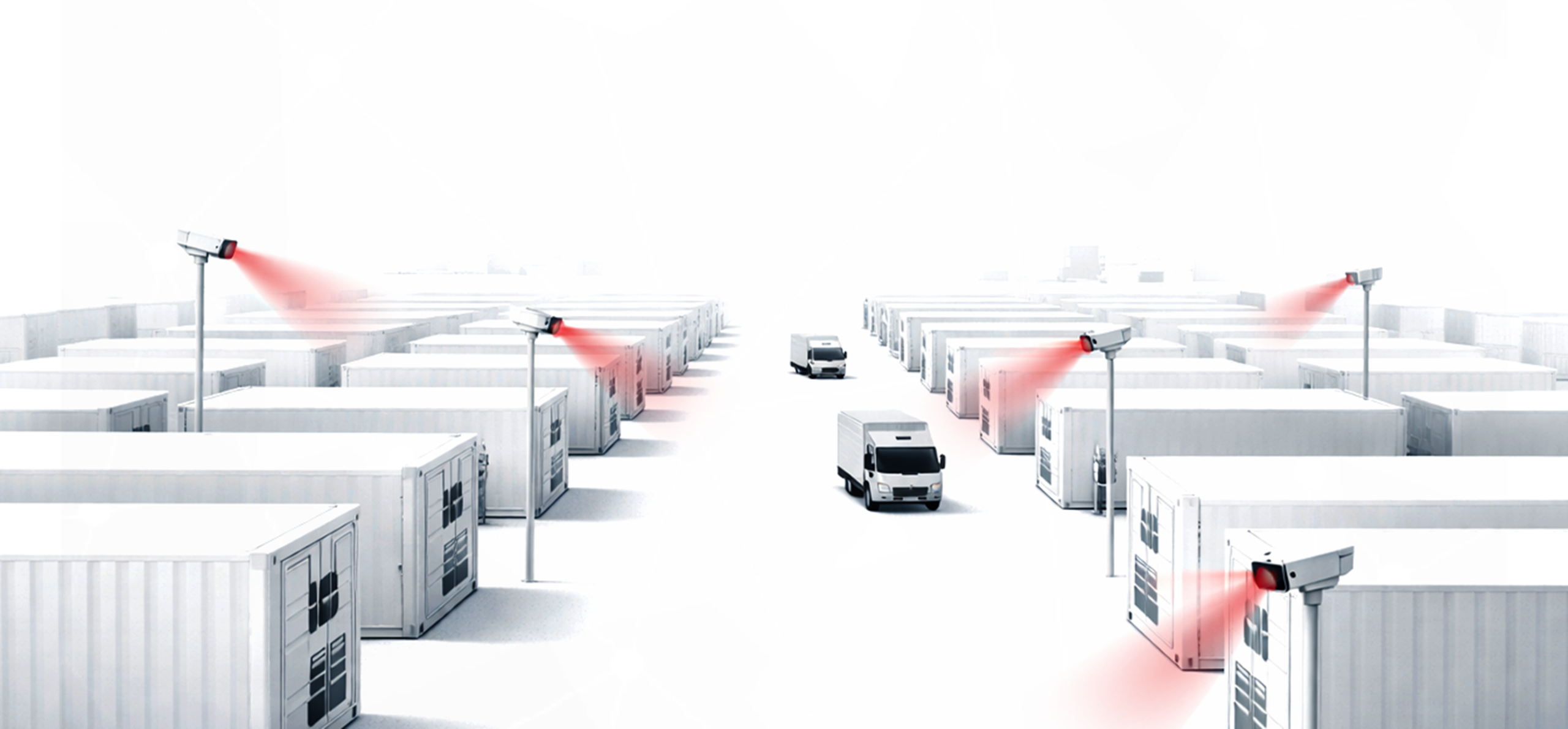
Busy container terminal at 6 AM. Trucks queuing at the gate, vessels berthing, yard equipment moving in every direction, and somewhere in the middle of all that organized chaos, a gate clerk squinting at a container number that’s half-obscured by road grime, trying to type it correctly into a system that will not forgive a […]

CEO & Co-founder
There’s a strawberry sitting in a warehouse in a port somewhere in Europe right now. It was picked three days ago. And if someone doesn’t know exactly what temperature it’s been kept at for the last 72 hours, that strawberry, and about 40,000 others just like it, might be quietly rotting. Nobody talks about that […]
CEO & Co-founder
At midnight, a high value shipment enters a regional logistics hub. By morning, the factory waited for those parts to halt production. The system shows the shipment as “received.” The yard team insists it was unloaded. The transporter says it left in perfect condition. No one is lying. No one can prove anything either. This […]
CEO & Co-founder
