Alignment And Overlay Accuracy
Nanometer Precision. Zero Overlay Errors. Layered Perfection Starts Here.
Nanometer Precision. Zero Overlay Errors. Layered Perfection Starts Here.
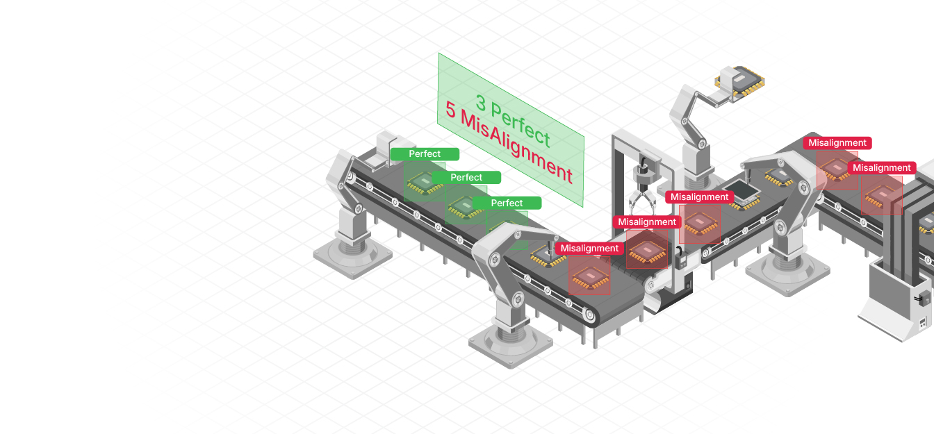
In semiconductor manufacturing, the success of multi-layer lithography depends on one thing: precision overlay. A nanometer-scale misalignment can trigger a cascade of failures, shorts, opens, or pattern mismatch. Traditional overlay systems, though reliable, are static and can miss real-time deviations.
AI-powered Alignment and Overlay Accuracy solutions use real-time computer vision to detect and correct misalignment during lithography. By continuously comparing new patterns with reference layers, AI vision ensures every overlay falls within strict tolerances, even on advanced nodes.
This reduces overlay-related yield loss, cuts rework cycles, and ensures multi-patterning integrity.

At advanced nodes (5nm/3nm), even tiny overlay shifts can cause electrical shorts or performance drift.

Thermal expansion or tool wear causes gradual shifts that traditional static calibration can’t catch.

Without real-time feedback, overlay errors often go unnoticed until after etching or metrology.

Multiple exposure passes increase the chance of cumulative misalignment, especially on dense layers.

Computer vision verifies overlay precision during exposure, not just in post-processing.

AI models trained to identify and measure overlay deviation at single-digit nanometer tolerances.

Learns and predicts overlay drift based on historical tool movement, exposure conditions, and material response.

Feeds deviation data into stepper/aligner systems for automatic compensation and dynamic realignment.

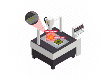
We begin by integrating CAD-based reference layers or GDSII data to set visual baselines for overlay comparison.
Specialized cameras with nanometer resolution are installed near lithography tools. Calibration includes pixel-level correction and motion compensation for fast-moving wafer stages.

Using archived mismatch incidents, our AI is trained to distinguish between acceptable variation and true overlay faults across complex geometries and resist layers.

As patterns are exposed, real-time visual feedback is compared to reference alignment. Detected deviation values are immediately sent to the scanner or aligner system for correction during the same pass.
Stay updated with the trending and most impactful tech insights. Check out the expert analyses, real-world applications, and forward-thinking ideas that shape the future of AI Computer Vision and innovation.
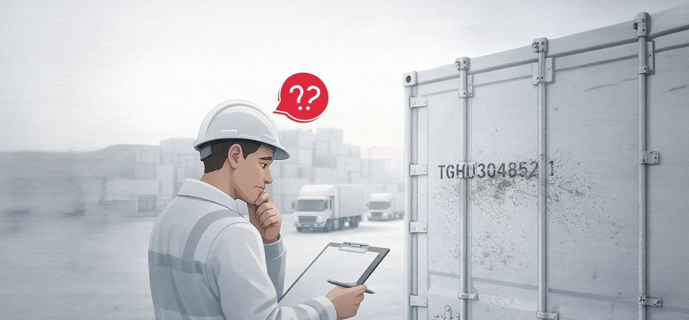
Busy container terminal at 6 AM. Trucks queuing at the gate, vessels berthing, yard equipment moving in every direction, and somewhere in the middle of all that organized chaos, a gate clerk squinting at a container number that’s half-obscured by road grime, trying to type it correctly into a system that will not forgive a […]

CEO & Co-founder
There’s a strawberry sitting in a warehouse in a port somewhere in Europe right now. It was picked three days ago. And if someone doesn’t know exactly what temperature it’s been kept at for the last 72 hours, that strawberry, and about 40,000 others just like it, might be quietly rotting. Nobody talks about that […]
CEO & Co-founder
At midnight, a high value shipment enters a regional logistics hub. By morning, the factory waited for those parts to halt production. The system shows the shipment as “received.” The yard team insists it was unloaded. The transporter says it left in perfect condition. No one is lying. No one can prove anything either. This […]
CEO & Co-founder
