
Customer
One of the Top 5 Steel Manufacturing Company in Japan
Project Details
- Duration: 3 Months+
Technologies:
- Deep Learning
- OpenCV
- PyQt
- Matplotlib
- SQLite
One of the Top 5 Steel Manufacturing Company in Japan
Technologies:
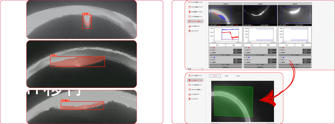
As the load cells are not installed in some furnaces, visual monitoring is performed by the operator.
We have designed a Desktop Application that performs the detection on the depleting area (Notch).
The Outcome: It is working with high accuracy, giving precise results and timely alerts.
Stay updated with the trending and most impactful tech insights. Check out the expert analyses, real-world applications, and forward-thinking ideas that shape the future of AI Computer Vision and innovation.
At midnight, a high value shipment enters a regional logistics hub. By morning, the factory waited for those parts to halt production. The system shows the shipment as “received.” The yard team insists it was unloaded. The transporter says it left in perfect condition. No one is lying. No one can prove anything either. This […]

CEO & Co-founder
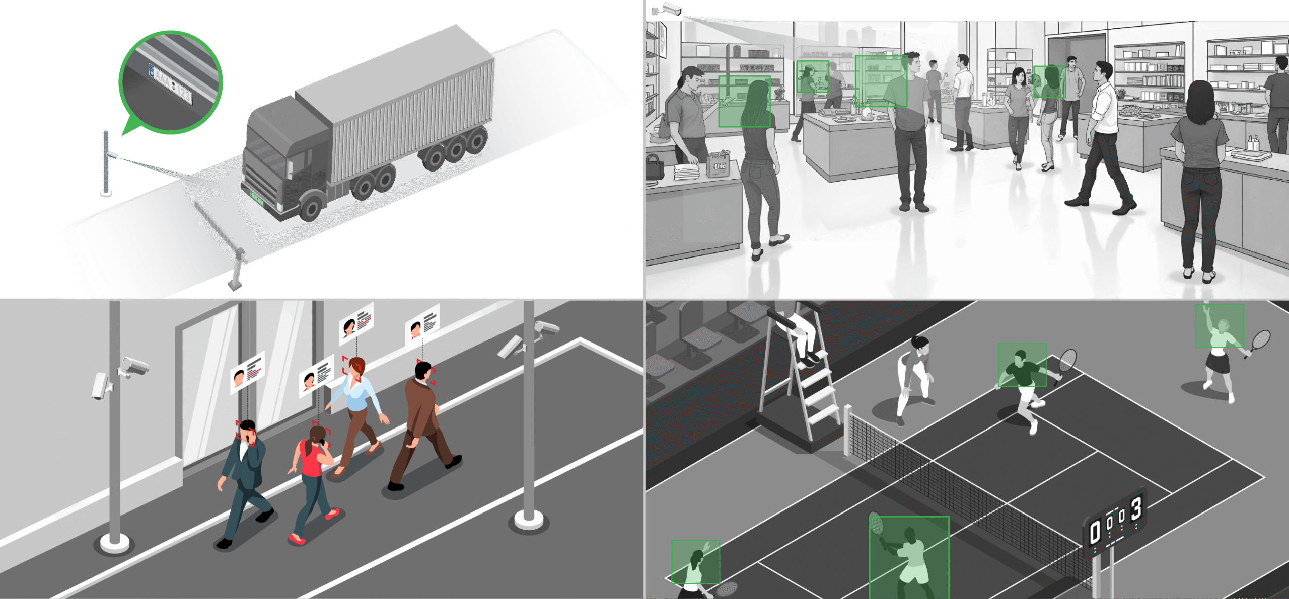
What ties these everyday moments together? It all looks connected… until you notice the pattern! Keep reading to know what? A truck entering a manufacturing campus. Crowds moving through a large exhibition hall. Containers rolling past a busy port gate. Players training across multiple tennis courts. Employees moving in and out of shared office spaces. […]
CEO & Co-founder
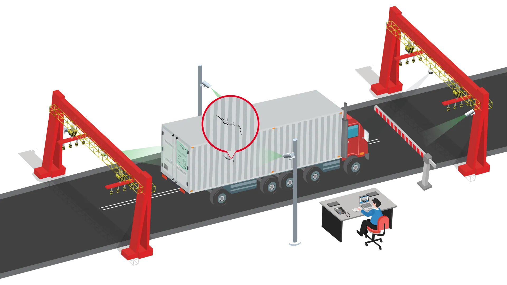
7:45AM at a busy automotive parts manufacturer. A delivery truck arrived at the dock. Usually, supervisors would take 10 minutes to scan paperwork. They’d also be keying in data. Instead, a camera quietly recorded the container ID, logged upon its arrival. And it tagged the shipment to a specific production line. All without a single […]
CEO & Co-founder
