How Computer Vision Is Transforming Semiconductor Fabrication Plants

Ruchir Kakkad
CEO & Co-founder
CEO & Co-founder
Semiconductor fabrication plants, commonly called fabs, are some of the most complex and expensive factories ever built. Inside cleanrooms that are thousands of times cleaner than a hospital operating room, wafers of silicon are transformed into chips that power the world’s smartphones, cars, medical devices, and satellites.
Every wafer goes through hundreds of steps, lithography, deposition, etching, polishing, packaging, and at each step, there is zero tolerance for mistakes. A single defect invisible to the human eye can multiply across millions of transistors and render an entire batch of chips useless. With advanced fabs costing billions of dollars to build and wafers worth thousands each, failure is not an option.
For decades, engineers relied on human inspection, microscopes, and rule-based automation to monitor wafers. But as technology nodes have shrunk from 90nm to 7nm, 5nm, and now 3nm, and with 2nm on the horizon, the old methods are no longer enough. Patterns are too complex, tolerances are too small, and the stakes are too high.
This is where computer vision in semiconductor manufacturing is changing the game. By combining ultra-high-resolution cameras with deep learning and automation, computer vision has become the new eyes of the fab. It enables real-time monitoring, faster decision-making, and higher accuracy than humans or legacy tools can achieve. From AI wafer inspection and overlay accuracy to CMP monitoring and packaging validation, vision based inspection is now at the heart of semiconductor automation.
Together, these technologies are giving rise to a new generation of smart fabs, factories that are not only faster and cleaner but also intelligent and adaptive.
To understand why fabs are embracing computer vision, we need to appreciate just how unforgiving semiconductor manufacturing is.
Each chip contains billions of transistors packed into a space smaller than a fingernail. A single defect, such as a scratch, a particle of dust, or a misaligned pattern, can cause a chip to fail. And because wafers are processed in lots, one defect can spread across hundreds of chips, costing millions of dollars in losses.
Photomasks, for example, act as the stencils for circuit patterns. If a photomask has a defect, that flaw is repeated across every wafer it prints. Similarly, if CMP polishing leaves a wafer slightly uneven, every subsequent layer is affected. If plasma etching goes too deep or too shallow, entire circuits may be ruined.
In short, precision is everything. And the smaller the node, the less room there is for error. This is why fabs are now investing heavily in semiconductor fabrication AI, to ensure that even the tiniest issues are caught and corrected before they cause large-scale yield loss.
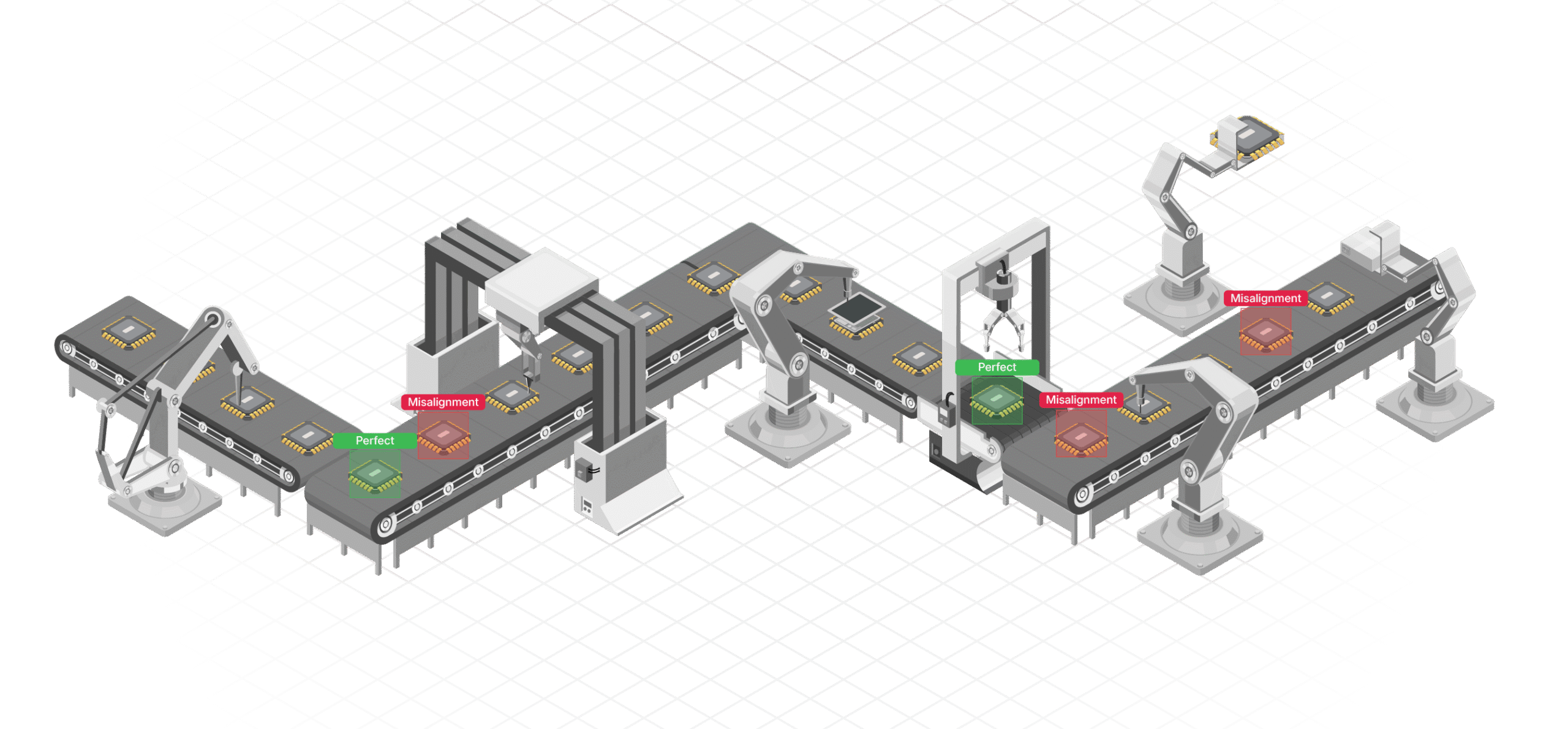
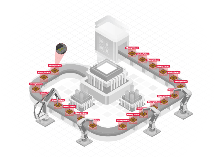
Computer vision is no longer limited to a single inspection step. It is now present across almost every stage of semiconductor manufacturing. Let’s explore the key areas where it makes the biggest difference.
Photomasks are the master blueprints for chips. Traditional inspections often missed defects at the sub-30nm scale. Now, AI-driven vision systems can scan masks at extreme resolution, catching defects like pinholes, scratches, or contamination before they spread to wafers. This improves yield and prevents costly rework.
As layers are stacked on top of one another, even a nanometer misalignment can cause electrical failures. Vision systems constantly monitor overlay accuracy, ensuring patterns line up perfectly. This is critical as fabs move to EUV (Extreme Ultraviolet) lithography, where tolerances are razor-thin.
CMP polishes wafers flat between layers, but it can also introduce dishing, erosion, and scratches. Vision systems analyze wafer surfaces post-CMP, detecting non-uniformity in real-time. This prevents defects from compounding across dozens of layers.
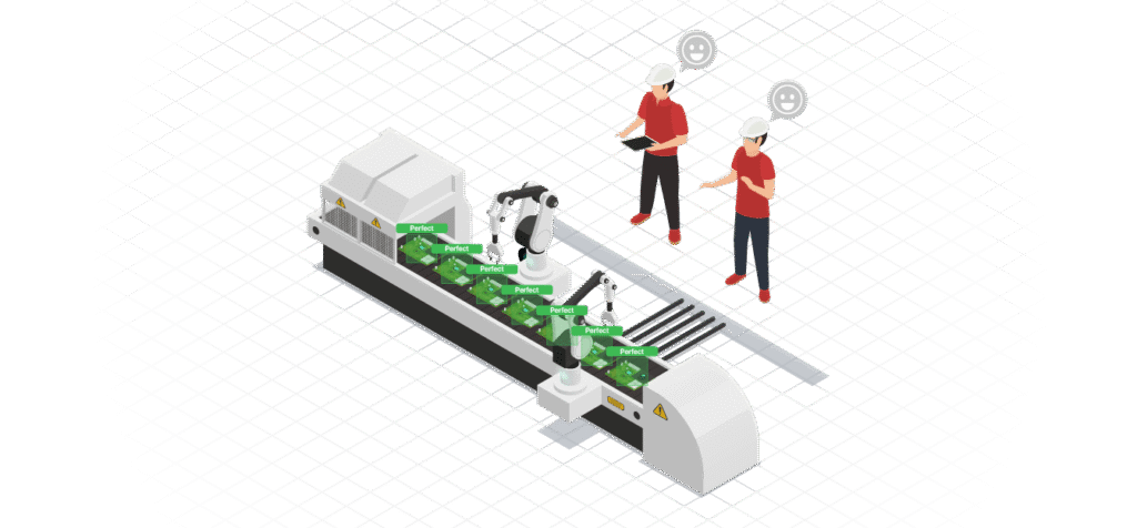
Once wafers are processed into modules or PCBs, vision systems check for open circuits, soldering faults, and missing components. AI wafer inspection at this stage ensures that packaging errors don’t undo the precision of earlier steps.
Etching defines the fine features of a chip, but stopping too early or too late can ruin circuits. Computer vision systems analyze plasma glow patterns in real time, ensuring etching ends exactly when it should.
Photoresist coating must be perfectly even. Vision-based inspection detects film thickness variations or surface contamination during coating, ensuring lithography accuracy.
In advanced packaging like Package-on-Package (PoP), vision systems ensure vertical alignment and connection integrity before reflow. This prevents latent defects that may only appear later in use.
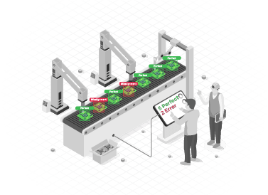
Instead of just flagging problems, modern vision systems categorize them, scratches, voids, pits, bubbles, so fabs can find root causes faster. This accelerates problem-solving and improves long-term yields.
Together, these use cases show how vision systems act as the silent guardians of fabs, watching every process, every wafer, every layer.
The impact of computer vision is more than just catching defects. It changes the economics and efficiency of semiconductor manufacturing.
One report suggests that fabs using vision based inspection and semiconductor fabrication AI have seen yield improvements of 20–30%, translating to hundreds of millions of dollars in savings each year.
The world’s leading fabs are already adopting these technologies.
In one case study, a fab that piloted AI-based CMP monitoring reported a 25% reduction in defect escapes and a 40% faster inspection cycle time. Another fab saw false positives drop by over 30%, freeing engineers to focus on real problems.
The analogy is clear: traditional inspection is like using a magnifying glass; AI-driven computer vision is like running an MRI scan. It sees deeper, faster, and with more context.
Adopting computer vision across fabs isn’t without hurdles.
Despite these challenges, the momentum is clear. The benefits far outweigh the barriers, and fabs are finding ways to integrate vision systems at scale.
The future lies in smart fabs, factories where vision systems not only detect defects but also correct processes automatically.
In short, computer vision is turning fabs from reactive factories into intelligent, semiconductor automation ecosystems.
At WebOccult, we understand that semiconductor fabs are under pressure like never before, shrinking nodes, tighter tolerances, higher costs, and massive demand. Our AI Vision solutions are built to help fabs navigate this challenge.
By combining expertise in computer vision in semiconductor manufacturing with deep industry knowledge, WebOccult delivers not just technology but a path to higher yield, lower costs, and smarter fabs.
The semiconductor industry has always balanced ambition and precision. As ambition drives us to smaller, faster, more powerful chips, precision becomes more unforgiving. At this level, a dust particle can be a villain, a scratch can be a disaster, and a single defect can cost millions.
Computer vision has become the watchtower of fabs. It ensures that defects are caught early, surfaces remain flat, patterns align perfectly, and packaging is precise. It turns fabs into smart fabs, intelligent, adaptive, and resilient.
In the race to advance Moore’s Law, computer vision in semiconductor manufacturing is not just a tool. It is the shield protecting yields, the compass guiding defect detection in chips, and the foundation of semiconductor automation.
At WebOccult, we are proud to help fabs take this leap. With AI-driven vision, we help manufacturers move closer to defect-free production, ensuring that every chip, every wafer, and every layer meets the standards of the future.