How AI-Powered Photomask Inspection is Driving Defect-Free Semiconductors

Ruchir Kakkad
CEO & Co-founder
CEO & Co-founder
The story of the semiconductor industry is the story of human ambition to make things smaller, faster, and more powerful.
We take this progress for granted when we buy a smartphone with a faster processor or a laptop with improved battery life, but behind these leaps lies an unforgiving pursuit of perfection at scales smaller than human vision can perceive.
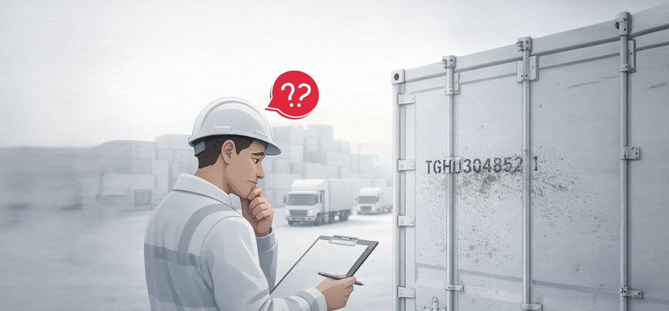
Among the many unseen heroes in this process is the photomask. It is not a finished chip, nor a shiny silicon wafer, but the stencil that defines how billions of transistors will be arranged on a wafer.
It is the master blueprint of the silicon age. If a photomask is flawless, the chips it produces will function with surgical precision. But if a photomask carries even a single microscopic defect, a tiny pinhole, a scratch, or a smudge of contamination, that flaw does not remain isolated. It is replicated over and over, across thousands of wafers, and multiplied into millions of faulty chips.
In an industry where one wafer lot can be worth millions of dollars, this is not merely a technical inconvenience. It is an existential threat to profitability and reputation.
For decades, photomask inspection has been the semiconductor industrys equivalent of a watchtower. Engineers peered into masks with high-powered microscopes and later relied on rule-based vision systems to catch anomalies. These methods were sufficient when chips were produced at 90 nanometers or 45 nanometers. But as we entered the age of EUV lithography and advanced nodes, 7nm, 5nm, 3nm, and now even the 2nm horizon, the task became impossibly complex.
This is the crucible in which AI-powered photomask inspection has emerged, not as a technology, but as a necessity. By combining ultra-high-resolution imaging with deep learning, AI systems have begun to see what human eyes and legacy machines cannot.
They identify defects invisible to traditional tools. They adapt as designs evolve. They reduce false positives that previously wasted precious engineering hours. Most importantly, they do all this at the scale and speed demanded by modern fabs.
To appreciate why AI matters, one must understand the financial and operational stakes. A single photomask set for an advanced node chip can cost more than a million dollars to produce.
Each mask defines a layer of the chip. And a chip at 5nm or 3nm can have over 80 layers, each dependent on the flawless integrity of its corresponding mask. If one mask is contaminated or scratched, the cascade is devastating. The cost is not limited to the replacement of the mask itself. Entire wafer lots are rendered useless, supply schedules are delayed, and in competitive markets like mobile processors or data-center chips, such delays can mean losing billions in market opportunity.
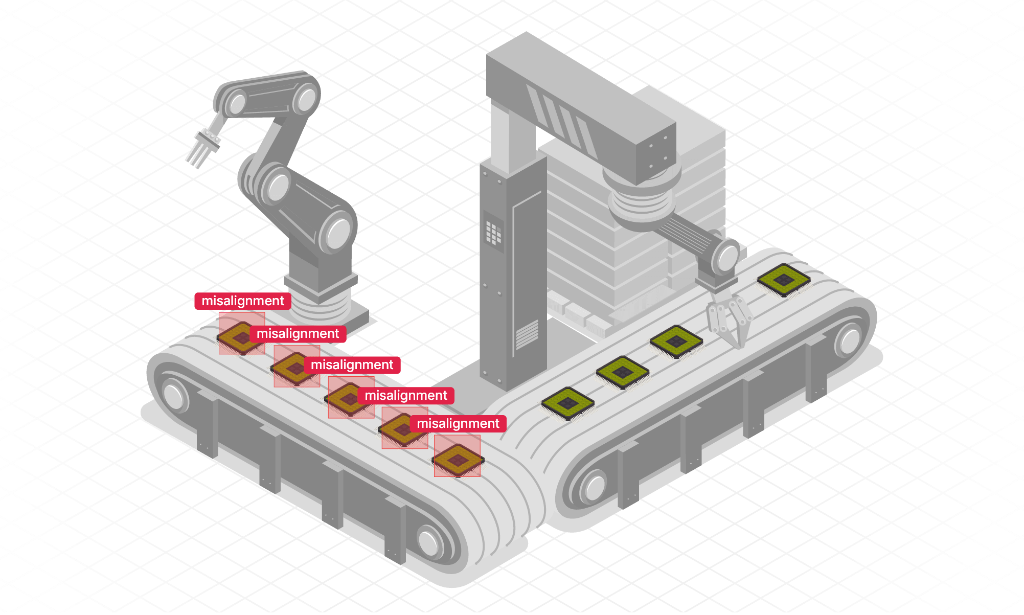
Defects take many forms. Some are simple pinholes, tiny transparent spots where chrome should block light. Others are scratches introduced during cleaning. Some are subtle distortions in line edges that only matter when shrunk to single-digit nanometers but can compromise transistor behavior at those scales. And there are contaminants, dust particles, residues, that alter light passage in unpredictable ways. Each is small enough to seem trivial, but each can merge into larger yield loss.
Industry studies suggest that defect-driven yield losses can reach up to 30% in advanced fabs. In a business where margins depend on extracting every usable die from every wafer, this is unsustainable.
The semiconductor industry cannot afford to rely on good enough inspection anymore. The need for perfection has become mandatory.
Photomask inspection, historically, relied on the principles of optical microscopy. Engineers magnified mask surfaces under intense light and scanned them for irregularities. Later, rule-based computer vision systems were introduced. These systems compared expected patterns against captured images, flagging possible defects.
But both methods had limitations. Optical systems cannot reliably resolve sub-30nm features, the very scale at which modern chips operate. Rule-based systems lack context. They cannot tell whether a deviation is a true defect or an acceptable variation, so they raise alarms indiscriminately. The result is an avalanche of false positives, forcing human engineers to waste time investigating harmless anomalies.
The complexity of patterns has also grown beyond human review. A single photomask may contain billions of features. Manually inspecting even a fraction of them is like asking a proofreader to check every letter in the largest library in the world without missing a single typo. No human can do it consistently. No rule-based system can adapt to the constant evolution of design complexity.
The industry has already felt the consequences. In 2019, a leading foundry reported significant production delays because a tiny particle contamination in photomasks went undetected during routine inspection. The defect replicated across wafers, causing tens of millions in yield losses.
Artificial intelligence changes the very nature of inspection. Instead of relying on rigid rules or limited optics, AI leverages pattern recognition at scale. It does not merely see, it learns.
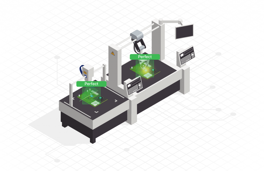
The process begins with ultra-high-resolution imaging. Photomasks are scanned at nanometer detail, producing massive datasets of images.
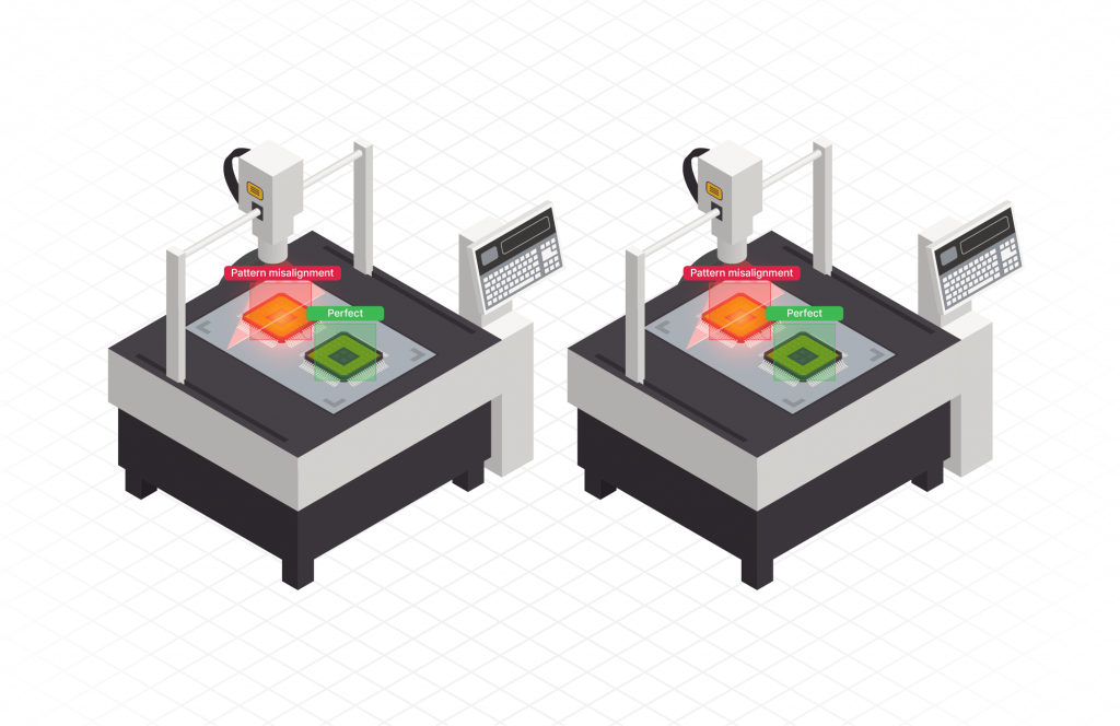
These images are then analyzed by deep learning models trained on millions of known defect and non-defect patterns. The AI distinguishes between a true defect and a harmless variation, something rule-based systems fail at.
Unlike traditional systems, AI is not static. With each inspection cycle, it adapts. New types of defects, new mask designs, new process variations, all become part of the AIs evolving intelligence.
What once required human engineers to redefine rules now happens automatically, continuously improving accuracy.
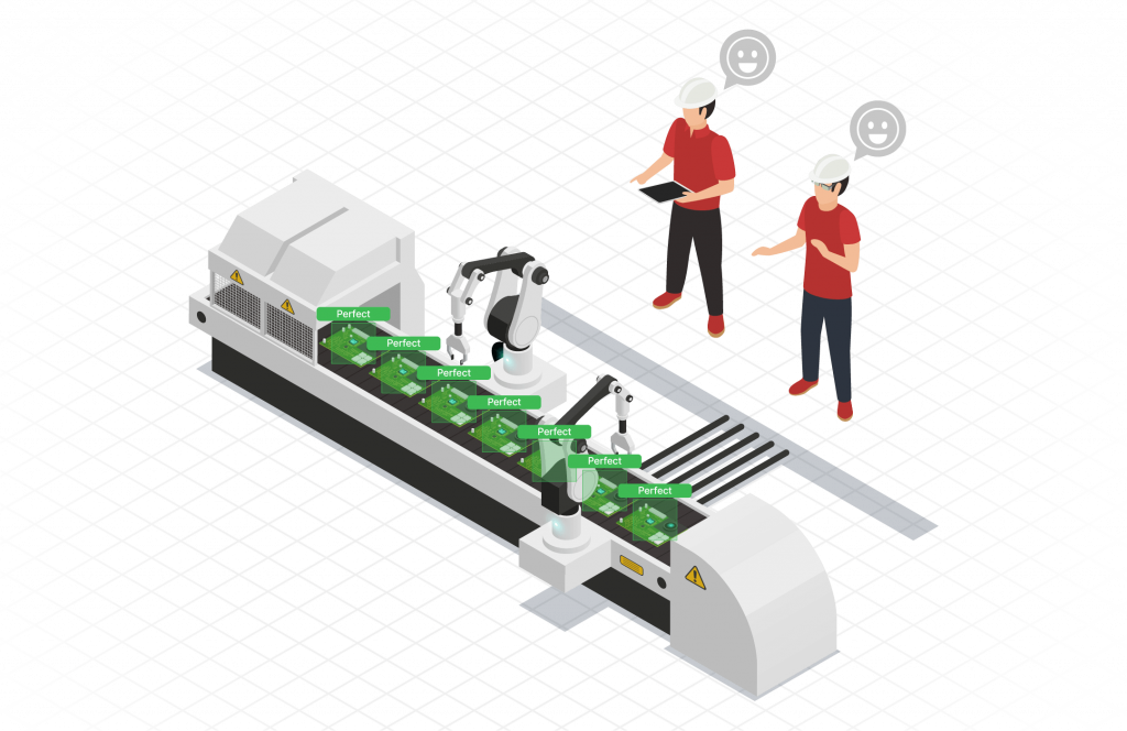
The results are transformative. AI-powered inspection achieves nanometer-level accuracy, detecting defects as small as 10-20 nm.
It reduces false positives dramatically, saving engineers from unnecessary reviews. It delivers results in real-time or near-real-time, enabling fabs to intervene before defective wafers are produced. In short, AI turns inspection from a passive checkpoint into a dynamic guardian of yield.
The benefits go beyond the fab ecosystem. First, there is speed. Fabs operate under heavy time pressure. Each minute of downtime translates into lost revenue. AI inspection accelerates throughput without compromising accuracy.
Second, there is consistency. Human inspectors tire. Rule-based systems miss context. AI, by contrast, delivers the same level of accuracy every time, across every mask, regardless of scale.
Third, there is scalability. As the industry pushes from 7nm to 5nm to 3nm and now 2nm, inspection challenges multiply. Traditional systems require constant reprogramming. AI, however, adapts seamlessly. The same architecture can inspect 28nm masks and 2nm masks, learning as it goes.
And finally, there is the financial impact. By preventing one defective photomask from replicating across thousands of wafers, fabs save millions in wasted materials and lost productivity.
McKinsey estimates that AI-driven defect detection can improve yields by 2030%, a staggering margin in an industry worth over half a trillion dollars annually.
This is not a theory, it is already happening. Leading fabs like Intel, Samsung, and TSMC are integrating AI-driven inspection into their workflows. Intel has spoken publicly about using deep learning to cut defect classification times dramatically. Samsung, in its push for 3nm Gate-All-Around technology, is believed to be using AI inspection to safeguard reliability.
The analogy is striking. Traditional inspection is like using a magnifying glass under sunlight. AI inspection is like using an MRI scanner, it penetrates beyond the obvious, revealing anomalies invisible to surface-level checks.
Yet, deploying AI is not without its challenges. Processing ultra-high-resolution mask images requires enormous computational power. This is why many fabs adopt hybrid models, combining edge computing near the equipment with cloud-based analytics for scale.
Data security is another concern. Photomasks embody some of the most valuable intellectual property in the world. Training AI models requires data, but fabs must protect design confidentiality. Secure frameworks and federated learning models are being explored to balance intelligence with protection.
AI also requires continuous retraining. As new defect types emerge and design patterns evolve, models must stay current. This demands ongoing data pipelines, collaboration between fabs and vendors, and an investment in infrastructure.
Finally, there is integration. AI inspection cannot exist in isolation. It must integrate seamlessly with lithography systems, manufacturing execution systems, and yield management platforms. The complexity is real, but so is the payoff.
The trajectory is unmistakable. AI inspection will soon be the standard, not the exception. As we march into the 2nm era and beyond, the industry cannot sustain defect detection through legacy means.
The future lies in self-correcting fabs, where inspection is not just a filter but a feedback loop. Defects will be detected in real time, and corrective actions, adjusting etch times, re-aligning patterns, modifying exposures, will happen automatically. Manufacturing lines will become self-healing systems.
AIs reach will also extend beyond photomasks. The same principles are already being applied to wafer inspection, CMP quality monitoring, plasma etching endpoint detection, and package assembly validation. Photomask inspection is simply the first frontier. The larger vision is AI-driven yield optimization across the entire semiconductor value chain.
At WebOccult, we believe that inspection is no longer about detection alone. It is about intelligence, adaptability, and integration. Our AI Vision solutions are designed not just to find defects, but to empower fabs with actionable insights. We focus on nanometer-level accuracy, deep learning-driven adaptability, and seamless workflow integration.
With proven expertise across industries as diverse as semiconductors, manufacturing, and automotive, we bring the versatility and reliability fabs needed in high-stakes environments. Our solutions are built for scale, engineered for security, and designed for the future.
For fabs navigating the challenges of advanced nodes, WebOccult offers more than a product. We offer a strategic advantage in safeguarding yield, reducing costs, and ensuring defect-free production at the cutting edge of technology.
The semiconductor industry has always been a dance between ambition and precision. As ambition drives us to smaller and faster chips, precision becomes ever more unforgiving. At this scale, dust particles become villains, and scratches become disasters. The photomask, as the master stencil of the silicon age, holds the power to make or break this pursuit.
AI-powered photomask inspection is not just a technological upgrade, it is the industrys guardian. It ensures that the invisible remains under control, that defects are caught before they replicate, and that fabs can continue the march of Moores Law without stumbling.
At WebOccult, we stand ready to partner with fabs on this path, bringing AI vision solutions that deliver precision, protect yield, and power the next generation of semiconductor innovation.