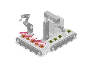
Lead Frame And Substrate Inspection
Inspect Before You Bond. Prevent Failure Before Assembly.

Inspect Before You Bond. Prevent Failure Before Assembly.

Lead frames and substrates form the physical base for semiconductor packages, any warpage, contamination, or dimensional fault at this level can cause bonding issues, electrical shorts, or total package failure. Manual inspection is inconsistent, and traditional 2D tools often miss warpage or multilayer misalignment. AI-powered Lead Frame and Substrate Inspection uses advanced 2D/3D computer vision to detect surface defects, warpage, and structural misalignment before die attach or wire bonding. With micron-level resolution and intelligent classification, the system ensures only flawless frames proceed to the next stage.

Scratches, dents, or oxidation on the lead frame surface may go undetected in visual checks, leading to bonding failure.

Substrate thickness, paddle depth, or pad spacing variations cause die misplacement or electrical mismatch.

Mechanical warpage due to improper storage or handling can cause poor die attach, especially in multi-layer substrates.

Human error and subjective judgment reduce reliability and throughput under high-volume demands.

Captures surface irregularities, corrosion, scratches, and dents using high-resolution visual and depth scanning.

Measures pad pitch, bond fingers, paddle flatness, and outline dimensions against golden specs.

Uses machine vision with 3D reconstruction to detect bending or structural warpage in substrates and frames.

Automatically classifies defects and routes defective units to rework bins or rejects them, no operator input needed.
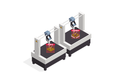

We begin by mapping the inspection point between cleaning and die attach stages, integrating the system with your substrate loader/unloader and frame handler.

Combining area-scan cameras and laser triangulation sensors, we enable full-surface and height-map acquisition for each lead frame or substrate in motion.

Our AI model is trained on real-world defect libraries from your past rejects, scratches, oxide marks, pad shifts, to achieve context-specific classification.

Inspection outcomes are sent to the MES (Manufacturing Execution System) in real time, triggering robotic sorters or binning logic to separate units by defect class or reworkability.
Stay updated with the trending and most impactful tech insights. Check out the expert analyses, real-world applications, and forward-thinking ideas that shape the future of AI Computer Vision and innovation.

Deepak runs operations at a mid-size terminal, and one number has bothered him for a month. Two ship-to-shore cranes, side by side. Same model, same year, same maintenance schedule. Crews rotate between them every shift. One averages 22 moves an hour. The other averages 30. He sends a maintenance team over the slow one. They […]

CEO & Co-founder

Pravin has run the empty depot for nine years, and he will tell you he knows every box in it. Then he walks you to the far corner, points at a container furred with dust, a small spider web in the corner casting, and goes quiet. It came in months ago. Nobody remembers the booking. […]
CEO & Co-founder

The morning shift supervisor, Imran, notices it before his first chai. A container in row C is sitting a few feet off its mark. Not knocked, not damaged. Just slightly wrong, the kind of wrong you only catch if you happened to see it the evening before. He checks the gate logs. Nothing after 22:00. […]
CEO & Co-founder
