Alignment And Overlay Accuracy
Nanometer Precision. Zero Overlay Errors. Layered Perfection Starts Here.
Nanometer Precision. Zero Overlay Errors. Layered Perfection Starts Here.
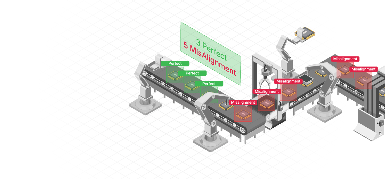
In semiconductor manufacturing, the success of multi-layer lithography depends on one thing: precision overlay. A nanometer-scale misalignment can trigger a cascade of failures, shorts, opens, or pattern mismatch. Traditional overlay systems, though reliable, are static and can miss real-time deviations.
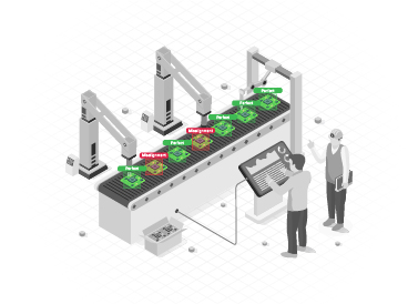
AI-powered Alignment and Overlay Accuracy solutions use real-time computer vision to detect and correct misalignment during lithography. By continuously comparing new patterns with reference layers, AI vision ensures every overlay falls within strict tolerances, even on advanced nodes.
This reduces overlay-related yield loss, cuts rework cycles, and ensures multi-patterning integrity.

At advanced nodes (5nm/3nm), even tiny overlay shifts can cause electrical shorts or performance drift.

Thermal expansion or tool wear causes gradual shifts that traditional static calibration can’t catch.

Without real-time feedback, overlay errors often go unnoticed until after etching or metrology.

Multiple exposure passes increase the chance of cumulative misalignment, especially on dense layers.

Computer vision verifies overlay precision during exposure, not just in post-processing.

AI models trained to identify and measure overlay deviation at single-digit nanometer tolerances.

Learns and predicts overlay drift based on historical tool movement, exposure conditions, and material response.

Feeds deviation data into stepper/aligner systems for automatic compensation and dynamic realignment.

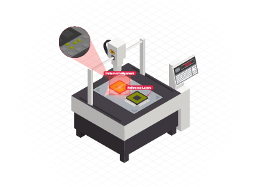
We begin by integrating CAD-based reference layers or GDSII data to set visual baselines for overlay comparison.
Specialized cameras with nanometer resolution are installed near lithography tools. Calibration includes pixel-level correction and motion compensation for fast-moving wafer stages.

Using archived mismatch incidents, our AI is trained to distinguish between acceptable variation and true overlay faults across complex geometries and resist layers.

As patterns are exposed, real-time visual feedback is compared to reference alignment. Detected deviation values are immediately sent to the scanner or aligner system for correction during the same pass.
Stay updated with the trending and most impactful tech insights. Check out the expert analyses, real-world applications, and forward-thinking ideas that shape the future of AI Computer Vision and innovation.
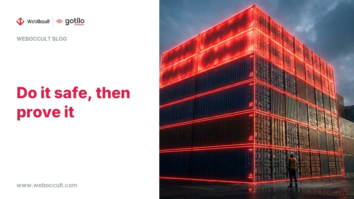
Three months after the incident, the assessor sits across from Meera, the operations manager, and slides a form over the desk. She is ready for questions about helmets, about whether the supervisor was present, about protocol. He asks none of them. He asks one thing instead: show me the footage. Meera’s yard runs safety well. […]

CEO & Co-founder
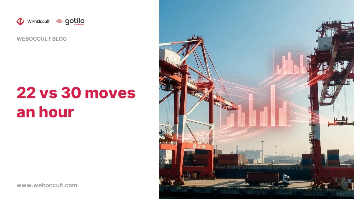
Deepak runs operations at a mid-size terminal, and one number has bothered him for a month. Two ship-to-shore cranes, side by side. Same model, same year, same maintenance schedule. Crews rotate between them every shift. One averages 22 moves an hour. The other averages 30. He sends a maintenance team over the slow one. They […]
CEO & Co-founder

Pravin has run the empty depot for nine years, and he will tell you he knows every box in it. Then he walks you to the far corner, points at a container furred with dust, a small spider web in the corner casting, and goes quiet. It came in months ago. Nobody remembers the booking. […]
CEO & Co-founder
