PHOTOMASK DEFECT INSPECTION
Catch Sub-Micron Errors. Preserve Pattern Integrity. Enhance Yield at the First Step.
Catch Sub-Micron Errors. Preserve Pattern Integrity. Enhance Yield at the First Step.
Photomasks are the blueprint of semiconductor manufacturing, and even the tiniest imperfection can lead to costly wafer defects across thousands of chips. Traditional manual and rule-based inspections are no longer viable for today’s advanced nodes. AI-powered Photomask Defect Inspection leverages ultra-high-resolution imaging combined with deep learning to detect sub-micron flaws like missing patterns, particles, scratches, or deformation, before they are replicated during lithography.

Human inspection or traditional rule-based systems struggle to catch nano-scale particles or structural flaws on masks.

High rejection rate of usable masks due to overly sensitive or static threshold systems.

Even when defects are detected, they are often not correctly categorized, slowing down root cause analysis.

Long inspection cycles and repeated mask validations delay exposure steps and increase cycle times.

AI models trained on vast defect datasets to detect and differentiate critical vs. non-critical anomalies.

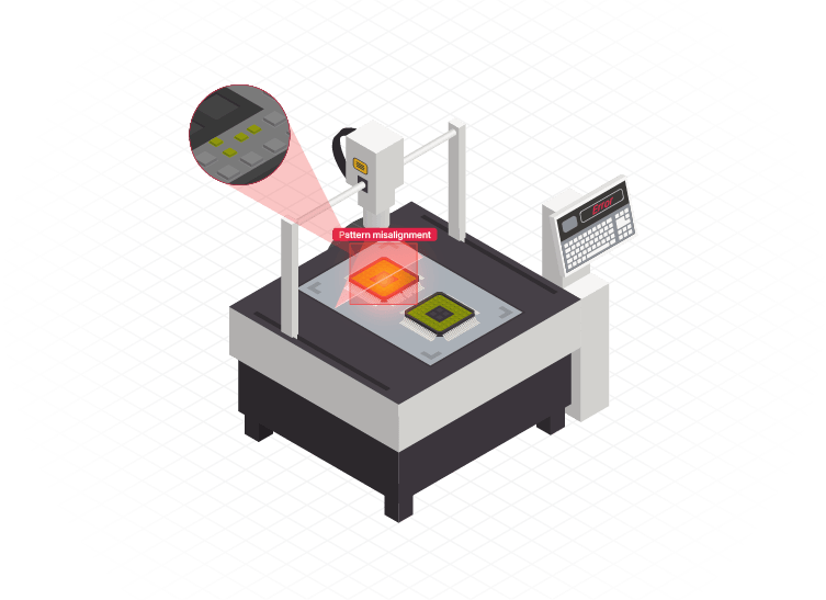
Micron and sub-micron precision imaging using specialized optics to catch the smallest pattern inconsistencies.

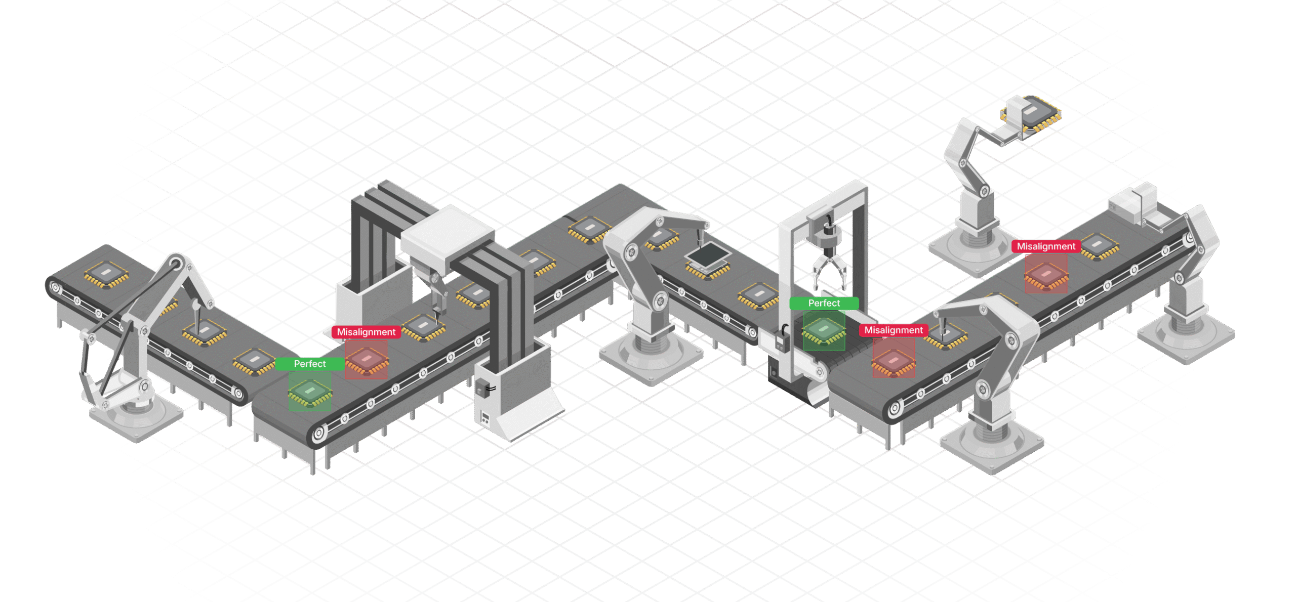
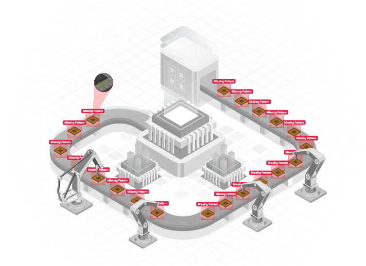
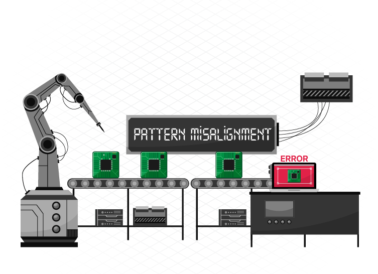
Classifies defect types (particles, scratches, edge defects, missing lines) and ranks them by severity and location.

Compares actual mask pattern with design files (GDSII) for pixel-level mismatch detection.

The system begins by ingesting GDSII design files of the intended mask layout. These files are used to create pixel-level reference patterns for comparison.

Specialized imaging systems are calibrated to achieve ultra-high resolution (sub-100nm) and correct for lens distortion, lighting uniformity, and reflectivity of mask surfaces.

Historical mask defect data, including particle types, line breaks, and haze, is used to train a defect classification model that distinguishes real issues from noise or permissible variations.

Captured images are analyzed frame-by-frame using AI models, and inspection results are displayed on an intuitive dashboard. Critical defects are flagged for review, while acceptable ones are auto-classified, reducing manual load.
Stay updated with the trending and most impactful tech insights. Check out the expert analyses, real-world applications, and forward-thinking ideas that shape the future of AI Computer Vision and innovation.

Three months after the incident, the assessor sits across from Meera, the operations manager, and slides a form over the desk. She is ready for questions about helmets, about whether the supervisor was present, about protocol. He asks none of them. He asks one thing instead: show me the footage. Meera’s yard runs safety well. […]

CEO & Co-founder

Deepak runs operations at a mid-size terminal, and one number has bothered him for a month. Two ship-to-shore cranes, side by side. Same model, same year, same maintenance schedule. Crews rotate between them every shift. One averages 22 moves an hour. The other averages 30. He sends a maintenance team over the slow one. They […]
CEO & Co-founder
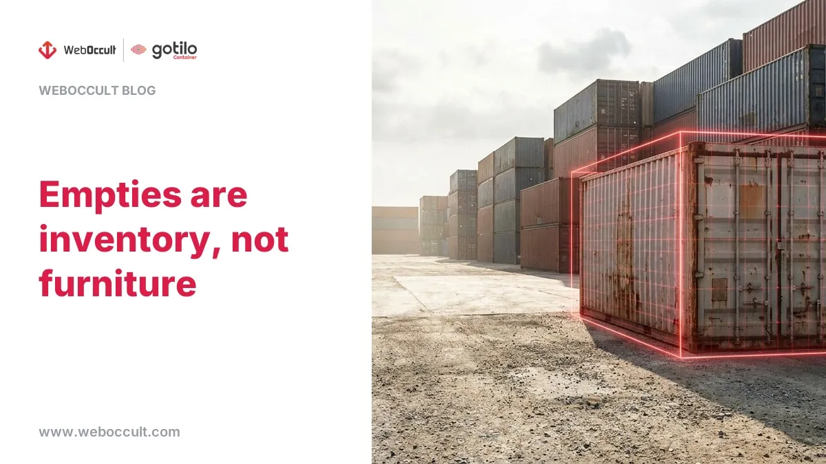
Pravin has run the empty depot for nine years, and he will tell you he knows every box in it. Then he walks you to the far corner, points at a container furred with dust, a small spider web in the corner casting, and goes quiet. It came in months ago. Nobody remembers the booking. […]
CEO & Co-founder
