
Customer
One of the Top 5 Steel Manufacturing Company in Japan.
Project Details
- Duration: 4 Months+
Technologies:
- OCR
- Machine Learning
- Python
- PyQt
- MongoDb
- Kafka
One of the Top 5 Steel Manufacturing Company in Japan.
Technologies:
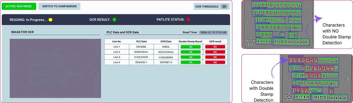
This 24X7 running company has assigned persons to verify the engraving on the Steel Plate by the Machine.
We have designed a Desktop Application that perform the OCR (Optimal Character Recognition) on the images.
Accuracy
Stay updated with the trending and most impactful tech insights. Check out the expert analyses, real-world applications, and forward-thinking ideas that shape the future of AI Computer Vision and innovation.
What Vision AI Can Actually See Let’s talk about the logistics industry’s strange addiction to buying new hardware. When confronted with a blind spot in the yard, our collective reflex is almost always to purchase another piece of plastic, attach a battery to it, and bolt it onto a steel box. We love sensors. We […]

CEO & Co-founder
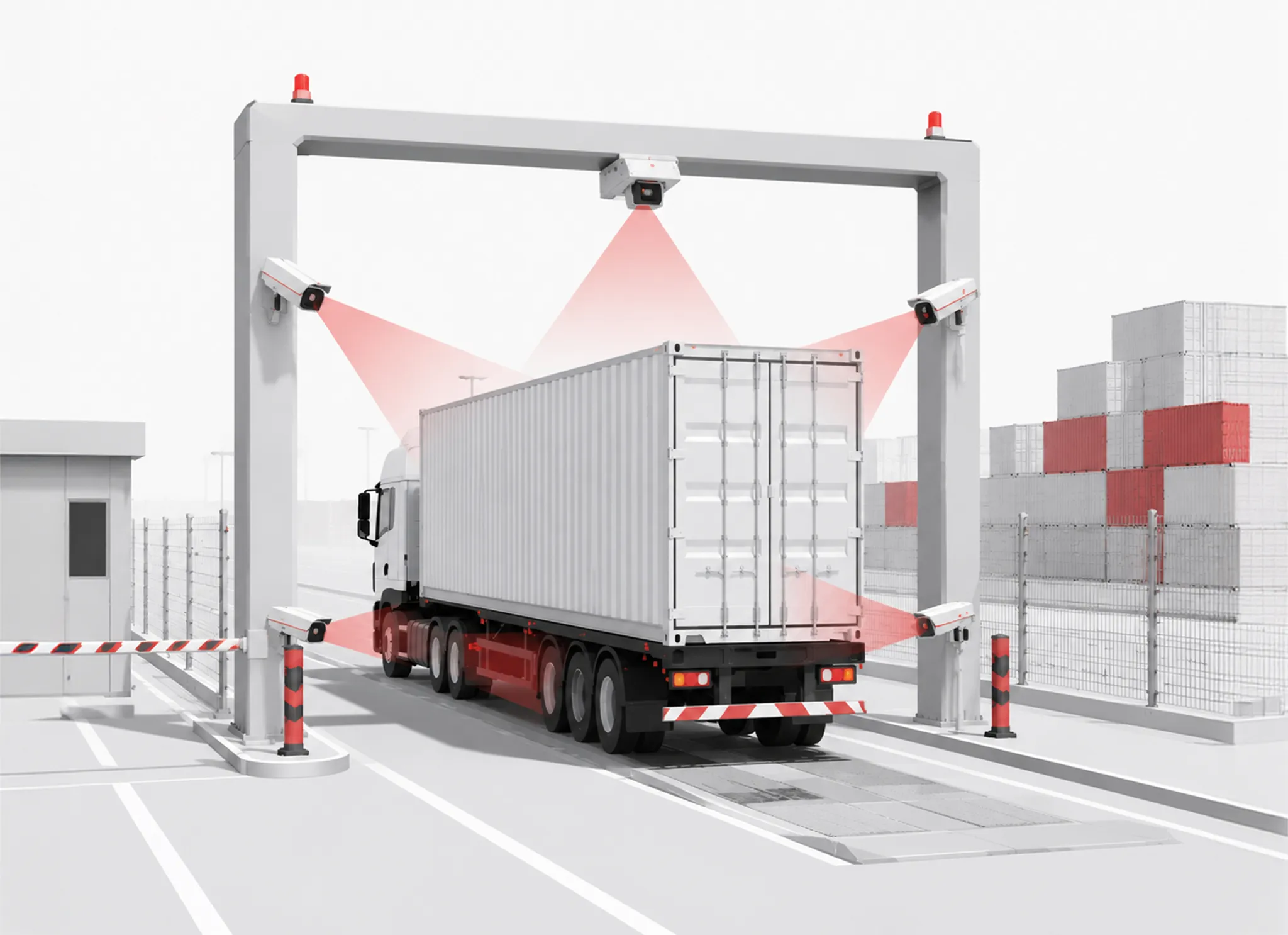
It usually arrives on a Tuesday morning. The subject line is aggressively vague, but the attachment tells you everything you need to know: a blurry photograph of a violently dented shipping container, accompanied by an invoice for the repair. Your terminal is officially being blamed for the damage. What follows is the most frustrating, time-consuming […]
CEO & Co-founder
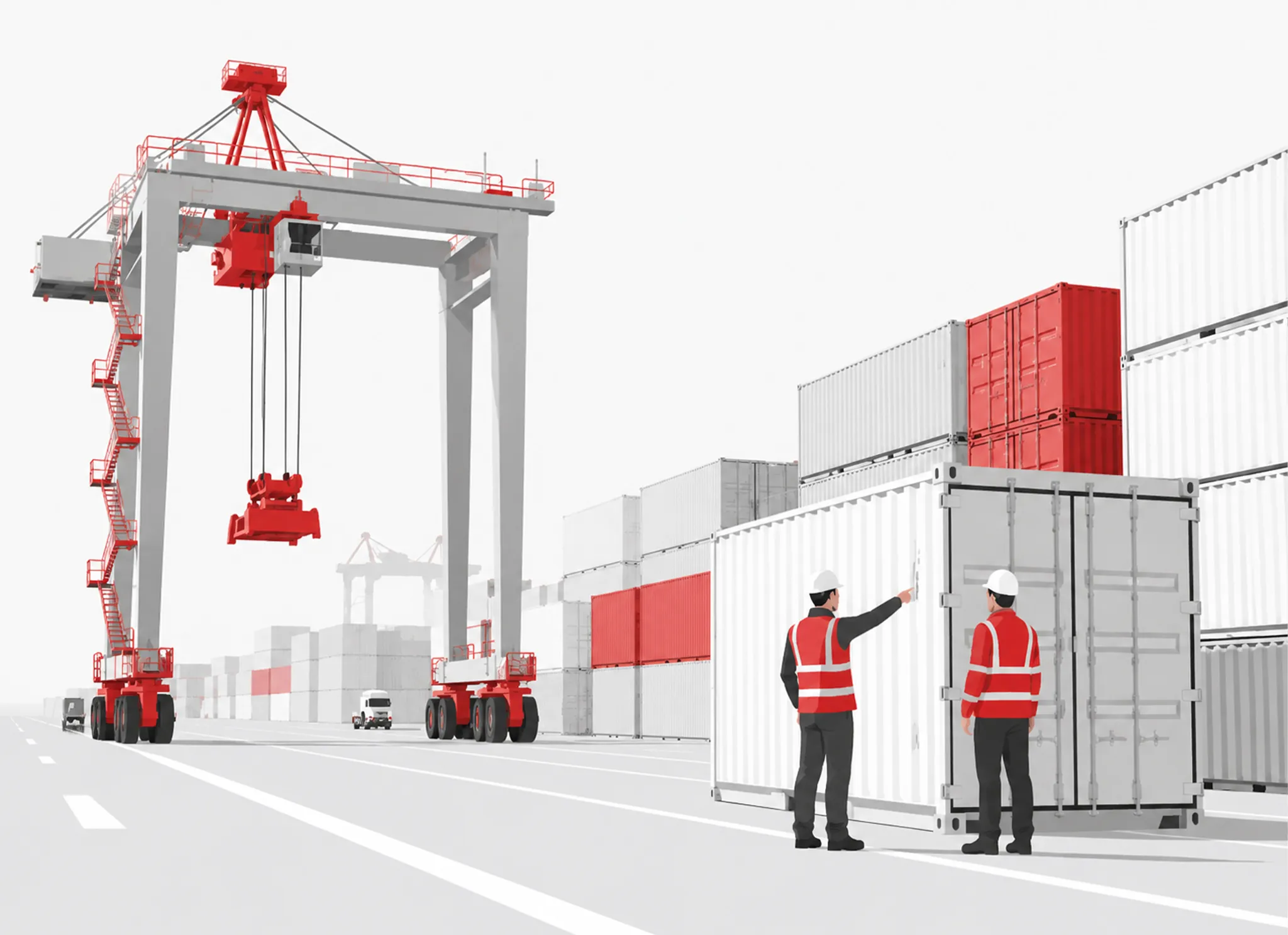
Let’s talk about the most terrifying event in terminal management: the retirement party. Every container yard has one. That veteran dispatcher or yard manager, let’s call him Frank. Frank operates with a battered clipboard, a radio held together by duct tape, and an encyclopedic mental map of five thousand identically rusted steel boxes. When a […]
CEO & Co-founder
